Following the design for manufacturing and design for assembly rules is essential for a quick transition from design to production. Overlooking these guidelines can result in fabrication setbacks, assembly defects, and longer turnaround times.
In this article, you’ll learn the most common DFM and DFA mistakes we see designers make, along with practical solutions to prevent them.
As a PCB engineer, knowing these errors will help you design production-ready boards.
Recurring DFM mistakes observed by our fab team
In this section, we cover DFM mistakes like unbalanced stack-up, trace and via design errors, wrong surface finishes, and overlooked manufacturing details.
1. Unbalanced stack-up
The PCB stack-up defines the board’s structure, thickness, and electrical performance. Poorly documented or unbalanced build-ups can result in fabrication delays, impedance mismatches, or mechanical problems such as warpage.
Typical design for manufacturing errors includes:
- Incomplete or unclear stack-up details, such as missing dielectric thickness, undefined copper weights, controlled impedance, or mismatched layer names between drawings and build-up files.
- Uneven copper distribution caused by asymmetrical routing, unbalanced dielectrics, or vague copper weight specifications leads to bowing or twisting during lamination or reflow.
- Final board thickness is calculated without accounting for copper plating, solder mask, or surface finish layers leads to discrepancies during fabrication.
Solutions:
- Provide a clearly labeled stack-up that includes all layers, copper weights, and dielectric thicknesses.
- Maintain symmetry in copper and dielectric layer distribution to reduce warpage risk.
- When calculating the final board thickness, remember to include the contribution made by copper plating, solder mask, and surface finish to the overall board thickness.
2. Trace design mishaps
Trace geometry, spacing, and routing directly affect signal integrity and current-carrying capacity of your board. Mistakes in trace design can result in electrical failures, EMI, or fabrication challenges, particularly in high-speed or high-current applications.
Common DFM mistakes include:
- Insufficient trace-to-trace or pad clearances in dense areas can cause shorts, etching defects, or unreliable solder joints.
- Unterminated traces (stubs) left on high-speed signal or power nets cause signal reflections and degrade signal quality.

- Inconsistent spacing between differential pairs disrupts impedance matching and introduces signal skew in interfaces like USB, HDMI, or LVDS.

- Copper routed too close to the board edge makes it vulnerable to: arcing, damage during depanelization, or copper exposure during edge plating.

- Varied copper weights on a single layer complicate PCB etching and often lead to over- or under-etched features.
- Missing teardrops at the pad/via junctions weaken the connection and increase the risk of trace lift-off during drilling or rework.
Solutions:
- Follow IPC-2152 guidelines for trace widths based on current requirements and allowable temperature rise.
- Make sure all the traces are connected to their respective endpoints.
- Maintain uniform spacing in differential pairs (3W).
- Add teardrops at all pad/via junctions to improve mechanical robustness.
- Incorporate a minimum copper-to-board edge clearance of 10 mil for outer layers and 15 mil for inner layers.
- Use consistent copper weights per layer and avoid mixing unless necessary and pre-approved.
3. Incorrect via design choices
Vias are essential for electrical interconnection in PCBs. Poor via design or documentation can lead to electrical failures, plating defects, or delays in fabrication.
Typical design for manufacturing defects includes:
- Insufficient annular ring due to tight drill-to-pad tolerances results in breakout or tangency.

- Inadequate spacing between holes causes drill damage or plating contamination.

- Vias placed too close to SMD pads lead to solder wicking and weak joints during reflow.
- Via-in-pad designs lacking proper filling or capping can create solder voids, tombstoning, or reflow defects.
- Missing via treatment specifications, such as via tenting and plugging, leads to exposed vias under components or contamination risks.
- Unclear blind via specifications.
Solutions:
- Maintain a minimum annular ring of 2 mil for laser-drilled vias, 3 mil for mechanically drilled vias, and 5 mil for component holes, and define anti-pad clearances on internal layers.
- Ensure a minimum clearance of 10 mil spacing between vias and routed or scored edges.
- Use filled and plated-over vias for via-in-pad applications, especially under BGAs or power components.
- Have a minimum 10 mil clearance between annular rings and adjacent copper pads to prevent shorts.
- Incorporate a drill-to-drill spacing of 8 mil.
- Specify via filling requirements following IPC-4761 in your fabrication notes and drill files.
- Work with your fabricator on blind and buried via configurations, use IPC-2221 standards, and ensure you have manufacturable stack-ups and achievable drill spans.
4. Solder mask design errors
The solder mask layer defines solderable and non-solderable regions of a PCB. It prevents solder bridging, oxidation, and electrical shorts. Errors in solder mask design can result in manufacturing defects, rework, or long-term reliability problems.
Common design for manufacturing errors include:
- Incorrect or missing solder mask openings where pads are covered or openings are misaligned, especially on BGAs or QFNs.

- No clearance around vias in copper pours leads to solder wicking during wave soldering and weak joints.
- Exposed traces under voids, such as via arrays, make them prone to corrosion, physical damage, or solder bridges.
- Gang solder mask openings make it difficult to inspect your boards and increase the risk of undesired connections.
Solutions:
- Follow IPC guidelines for solder mask-to-pad clearance (1.6 mil) and mask dam width (4 mil).
- The ratio between solder mask openings and pad size should be 1:1.
- Tent or cover vias in copper pours as needed to prevent solder wicking.
- Avoid large gang mask openings; define individual openings for each pad when possible.
5. Unclear silkscreen text
Silkscreen conveys critical assembly and inspection information, including reference designators, polarity marks, and component outlines. Improper silkscreen design can lead to poor legibility, soldering defects, and assembly errors.
Typical design for manufacturing errors includes:
- Unclear or blurry silkscreen text.
- Overlapping silkscreen with pads or copper features.

- Poor contrast between silkscreen ink and solder mask reduces readability during inspection and manual assembly (e.g., red on black, yellow on white).
- Missing component outlines or orientation marks, such as a pin 1 indicator, causes part misplacement, especially for polarized components.
Solutions:
- Use high-contrast silkscreen and solder mask combinations such as white on green.
- Maintain at least 4 mil clearance between the silkscreen and pads or vias.
- Ensure all text is sized for legibility and remains readable after solder mask and printing processes.
- Include clear component outlines and orientation markers.
- Run silkscreen-specific DFM checks to flag overlaps, missing markings, or size violations.
- Provide a minimum line width of 5 mil and text height of 25 mil for better readability.
6. Incompatible surface finish selection
Surface finish is a protective layer on a PCB applied to prevent oxidation and ensure good solderability during component assembly. It also affects the board’s performance, reliability, and shelf life.
Choosing the wrong finish or providing unclear requirements finish requirement in the fab notes can lead to solder defects or tarnish.
Common design for manufacturing errors include:
- Unspecified or incompatible finishes in the fab notes lead to incorrect use of coatings that are not suited for the board’s requirements, such as HASL under BGAs or OSP in humid environments.
- Inconsistencies between the fab drawing and the manufacturing process flow can lead to the wrong layer sequence. For instance, if the surface finish is specified before the solder mask layer in the stack-up drawing, it would lead to a faulty layer arrangement as shown below. The right sequence is surface finish after solder mask coating.

Solutions:
- Clearly specify the surface finish type (e.g., ENIG, HASL, OSP) along with the required thickness, referring to IPC-4552 or applicable finish-specific standards.
- Ensure consistency between fabrication notes, stack-up drawings, and manufacturing flow to avoid conflicts.
7. Overlooked mechanical constraints
Mechanical features like board outlines, cutouts, slots, and cavities must be precisely defined in the fab notes. Missing or ambiguous details can cause incorrect routing, inaccurate/missing plating, or incomplete machining, impacting mechanical fit and board functionality.
Typical design for manufacturing mistakes include:
- Insufficient clearance between the V-score and copper features increases the risk of board damage during depanelization.
- Unspecified plating for slots or cutouts results in non-conductive ground shields, connector failures, or signal path interruptions.
- Missing or unclear depth milling instructions where Z-axis dimensions for cavities, counterbores, or partial-depth slots are not defined in fabrication or mechanical drawings.
- Ambiguous or unmarked internal features, like cutouts or slots, are shown only in copper or silkscreen layers without clear callouts in your fab drawing leads to manufacturing errors.
- Overly tight or missing tolerances on board outlines, drills, slots, and mechanical cutouts increase fabrication cost.
Solutions:
- Maintain a minimum of 15 mil clearance between V-score and copper features.

- Define all mechanical features, board outline, slots, cutouts, and cavities on a dedicated mechanical layer.

- Specify plating requirements for all slots and edge connectors in the fab notes.
- Include complete Z-axis definitions for any depth-milled features and reference them consistently across drawings and documentation.
- Follow your manufacturer’s tolerances for mechanical features.
8. Missing or wrong information in production files
Accurate and complete production files are critical for PCB fabrication. Discrepancies between design data and fabrication instructions can result in delays. The most common problems arise from mismatches across Gerber/ODB++ files, drill data, fabrication drawings, and netlists.
Common design for manufacturing errors include:
- Inconsistent Gerber data and fab notes, such as missing silkscreen or drill layers, differing layer count.
- Drill file inconsistencies, including incorrect origins, unit mismatches, or missing vias.
- Ambiguous fabrication drawings, where board dimensions, stack-up details, or copper weights are unclear.
- Missing or incompatible IPC-D-356A netlists make it difficult for fabricators to verify electrical connectivity.
Solutions:
- Review the complete CAM output to ensure all required files are present and correctly formatted.
- Include all essential production files: Gerber/ODB++/IPC-2581, NC Drill, fabrication drawing, and IPC-D-356A netlist.
- Verify internal consistency across all files, check for matching units, origins, layer count, and naming conventions.
- Ensure fabrication drawings are complete and unambiguous. Clearly define board dimensions, stack-up, copper weights, and hole specs.
- Run a DFM check considering your manufacturer’s capability.
- Use a standardized file naming structure and avoid generic names like “Layer1” or “Top”.
Download our eBook for more design for manufacturing tips.

Design for Manufacturing Handbook
11 Chapters - 96 Pages - 90 Minute ReadWhat's Inside:
- Annular rings: avoid drill breakouts
- Vias: optimize your design
- Trace width and space: follow the best practices
- Solder mask and silkscreen: get the must-knows
Download Now
Recurring DFA mistakes observed by our assembly team
In this section, we highlight common DFA issues such as footprint and part placement mistakes, soldering errors, cleaning and coating oversights, and process compatibility gaps.
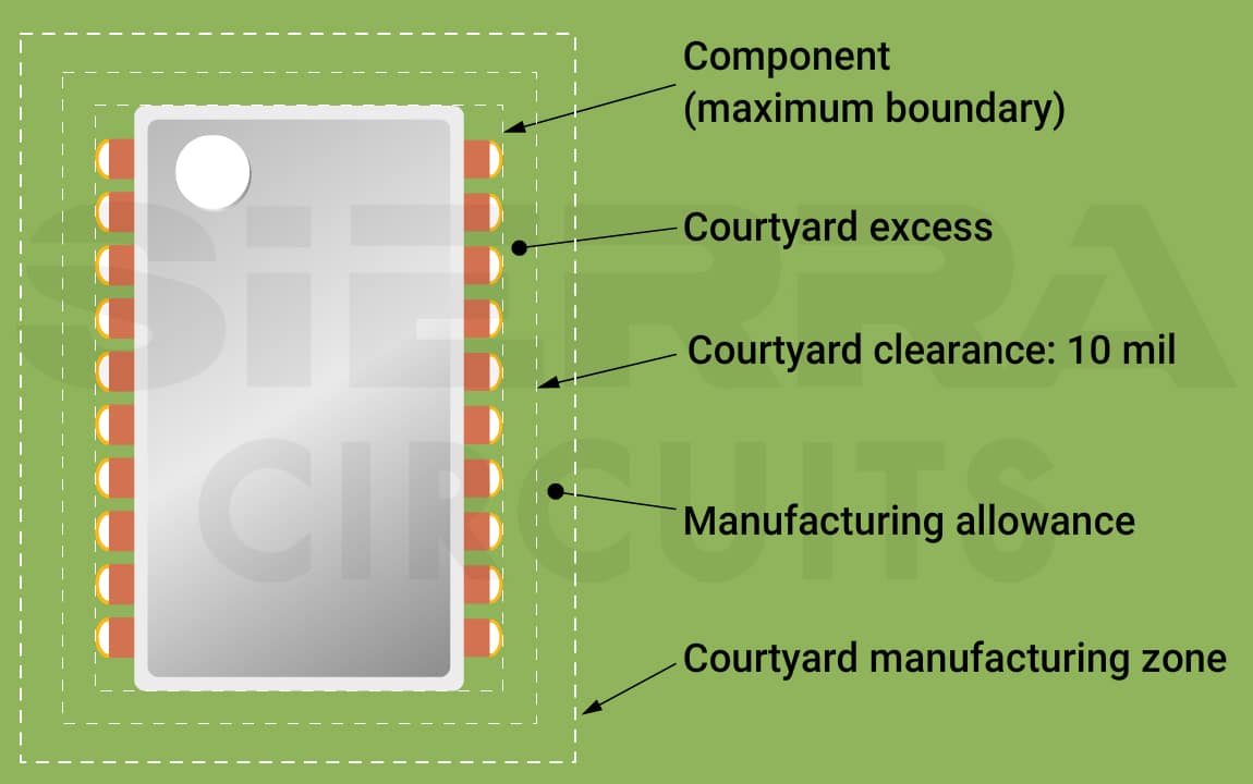
1. Incorrect component footprints and placement
Precise component placement and footprint design are critical for an efficient PCBA. Poor placement or inaccurate land pattern can lead to clearance violations, misalignment, and soldering defects.
Common design for assembly errors include:
- Placing components too close to board edges, test points, or each other causes clearance issues during assembly or depanelization.
- Insufficient component to annular ring clearance.
- Incorrect, duplicate, or missing reference designators.
- Mismatch among silkscreen, BOM, and pick-and-place file data.
- Non-standard or inaccurate footprints where the pad size or pitch does not match the part datasheet.

- Misaligned polarity markings or pin 1 marking for polarized components.

- Incorrect orientation of polarized components.
- Courtyard violations limit space for part placement, inspection, or rework.
- Conflicting component heights obstruct the placement tools or affect coating and inspection quality.
- Inadequate spacing for pick-and-place machines leads to placement errors when fine-pitch components are placed near tall parts or dense arrays.
- Missing alignment marks cause pick-and-place and AOI misregistration, especially for BGAs and fine-pitch ICs.
Solutions:
- Follow IPC-7351 guidelines for keep-out zones, courtyards, component spacing, and land pattern design.
- Maintain a minimum spacing of 7 mil between the component pad’s edge and the edge of the annular ring.

- Check reference designators and part orientation across schematic, BOM, silkscreen, and pick-and-place files.
- Use OEM-recommended footprints.
- Ensure polarity and pin 1 indicators are clear in both silkscreen and assembly documentation.
- Group components by height and incorporate clearance zones around tall parts as per your assembly vendor guidelines.
- Maintain minimum clearances between components and board edges, test points, or tooling holes to prevent damage and allow proper access during assembly.
- Adhere to component spacing as per IPC-2221 or specific assembly requirements to prevent soldering defects.
- Provide at least 3 global fiducials and 2 local fiducials for large ICs or BGAs, free from nearby copper, and define them in the paste layer.

Sierra Circuits performs a thorough design for assembly analysis to ensure error-free PCBAs. To learn more, see our PCB assembly capabilities.
2. Improper reflow considerations
Reflow soldering demands thermal balance and component stability. If your design lacks symmetry in pad sizes, copper areas, or component placement, it can cause tombstoning, shadowing, or poor solder joints.
Typical design for assembly errors includes:
- Placing components on both sides of the PCB increases reflow costs and raises the risk of bottom-side part displacement during the second reflow cycle.
- Thermal imbalance in board layout causes tombstoning and shadowing in small component packages like 0402 or 0201.
- Absence of thermal reliefs on wave-soldered through-hole pads leads to incomplete soldering.
Solutions:
- Place small, lightweight components on the bottom side and heavy/tall parts on the top side of your printed board.
- Implement symmetrical copper connections and ensure consistent solder paste volumes to avoid tombstoning and shadowing.
- Use thermal relief connections for through-hole pins connected to large planes to ensure solderability and reduce cold joints.
- Validate thermal profiles using simulations or trial runs to ensure uniform heat distribution during reflow.

3. Ignoring the solder paste layer and flux compatibility
Soldering success relies on the correct use of paste data, aperture design, and flux selection. Designers often miss key paste layer details or misapply flux types.
Common design for assembly errors include:
- Omitting the solder paste layer from the Gerber output or forgetting apertures on essential SMD pads.
- Adding paste openings on non-pad areas like test points or silkscreen.
- Selecting incompatible flux types leaves corrosive residues behind after cleaning.
- No clear mention of assembly type (RoHS vs. leaded). This increases the risk of using the wrong alloys.
- No bake-out instructions for moisture-sensitive parts (e.g., MSL level 3+) increase the risk of popcorning during reflow.
Solutions:
- Include a validated solder paste layer (e.g., GTP for top side) and ensure every SMD pad has an appropriately sized aperture. Remove unnecessary paste features and avoid merged apertures between fine-pitch pads.
- Specify the flux type in the assembly notes and match it with the intended cleaning method (e.g., no-clean vs. water-wash).
- Mention soldering requirements (RoHS or leaded) and include baking guidelines in the assembly document.
4. Skipping cleaning and coating instructions
Post-solder cleaning and conformal coating are often neglected during the design phase. This may cause long-term corrosion, electrical leakage, or testing difficulty.
Typical design for assembly errors includes:
- Undefined cleaning process or flux classification causes process mismatch (e.g., washing no-clean flux with water).
- Missing conformal coating instructions results in coating over connectors, test points, or keep-out zones.
Solutions:
- Specify flux classification (e.g., ROL0, ROM1) and compatible cleaning processes in the assembly documentation.
- Define coating material, masking strategy, and areas to avoid (e.g., connector pins, test pads) in the fab and assembly notes.
5. Overlooking the component lifecycle
Failing to consider traceability and component availability at the design stage can delay production.
Common design for assembly errors include:
- Not mentioning the requirement for traceability or certificates of conformance (COC) leaves suppliers unsure of documentation expectations.
- Specifying obsolete or end-of-life (EOL) parts leads to last-minute substitutions.

Solutions:
- Include traceability and COC expectations in purchase orders and documentation, especially for aerospace, medical, or automotive projects.
- Regularly check BOM using supplier databases.
Understanding and avoiding common design for manufacturing and design for assembly mistakes can reduce rework, prevent delays, and minimize manufacturing costs. By incorporating these guidelines into your next PCB design, you can ensure efficient fabrication and assembly processes, saving both time and money while delivering a reliable end product.
Download our design guide to learn more about design for assembly.

Design for Assembly Handbook
6 Chapters - 50 Pages - 70 Minute ReadWhat's Inside:
- Recommended layout for components
- Common PCB assembly defects
- Factors that impact the cost of the PCB assembly, including:
- Component packages
- Board assembly volumes


