What is design for manufacturability for PCBs?
DFM rules for a PCB is a set of guidelines that ensure the manufacturability of a circuit board. In order to be manufacturable, the design should meet the fabricator’s capabilities, such as trace width, trace to copper, drill size, board edge to copper, and blind/buried via.
What happens when you ignore your manufacturer’s capabilities
We have noticed designers design their boards without considering their manufacturer’s capabilities. When such design files are sent for fabrication, the manufacturer will run a check, notify you about the DFM issues, and will wait for further instructions. Consequently, you will have to modify your design to ensure it can be fabricated easily. This redesign can be time-consuming and expensive.
This is why it is important to know your fabricator’s capabilities in advance. Implementing DFM rules will minimize or eliminate board respins by ruling out layout changes, redesigns, and re-validation of board functionalities.

What is DFM analysis?
DFM analysis is a process that evaluates the PCB layout to minimize problems that may be encountered during the manufacturing and assembly processes.
In the CAD tool, the constraints for manufacturing are entered. For example, if the manufacturer can fabricate a minimum trace width of 3 mils, the constraints in the tool for minimum trace width are set to 3 mils. Wherever the traces are less than 3 mil, this tool will indicate an error as a part of the design rule check.
Here’s a quick overview of design for manufacturing standards you need to know for an error-free PCB.


Design for Manufacturing Handbook
11 Chapters - 96 Pages - 90 Minute ReadWhat's Inside:
- Annular rings: avoid drill breakouts
- Vias: optimize your design
- Trace width and space: follow the best practices
- Solder mask and silkscreen: get the must-knows
Download Now
Files required for fabrication
One of the first DFM rules to follow is to check whether all the files required for manufacturing are provided.
- Gerber/ODB++ files
- NC drill file
- IPC 356A netlist
- Component placement file (pick and place)
- PDF files – (assembly files, fab details, and schematic)
DFM checks for drill holes
Drilling is the first manufacturing step towards making a via that serves as a vertical connection between different board layers. This is the most expensive, laborious, and irreversible process. This is carried out after the lamination cycle.

The chart below lists a few drill checks that identify the potential manufacturability defects:
| Drill checks | Objective |
|---|---|
| Missing holes | To Identify missing drills for non-SMD pads |
| Duplicate holes | To identify drills that are not assigned to any pad |
| Stubbed vias | To report vias that aren't connected to at least two copper layers |
| Hole spacing | To determine touching holes or close holes |
The drilling process has two major aspects to be considered:
Aspect ratio
The aspect ratio (AR) is the proportion of the drill depth to the drilled hole diameter.
The AR for through-hole is given by:
(Thickness of the PCB) / (Diameter of the drilled hole)
Typical AR for through-holes is 1:10 (for a 62-mil thick board)
The aspect ratio for microvias is given by:
[Drill depth (h)] / [Diameter of the drilled hole (a)]
AR for microvias = 0.75:1

Drill-to-copper
Drill-to-copper is the land clearance between the drilled hole edge and the nearest copper feature. The nearest or closest copper feature can be anything ranging from a copper trace, pour, or other similar active copper regions.
The finished hole to copper clearance will be the drill to copper clearance, which includes the copper plating thickness. A finished hole is a hole obtained after metallization and surface finish.
Finished hole to copper clearance = drill to copper clearance + (plating thickness x 2).
So if the drill diameter is 6 mil and the plating thickness is 1 mil, then the finished hole to copper clearance = 6 + 1 x 2 = 8 mil.
For drill-to-copper, always the drilled hole edge is considered.

Insufficient or improper annular ring width can lead to the following issues:
- Tangency – Annular ring touching the edge of the pad
- Breakout – Annular ring coming out of the pad
To learn the difference between DRC and DFM, see design rule check vs. design for manufacturing.
DFM signal checks
Signal checks are performed as soon as the Gerber files are received. This checklist contains critical parameters, including conductor width, hole registration, spacing requirements, and many more.
Conductor width

The conductor width is the width of the trace ‘W’, as shown in the figure above.
The formula for trace width calculation for allowable current as per the IPC-2221 standard is given as:

The cross-sectional area A is calculated using the formula given below:
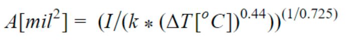
For internal layers k = 0.024 and for external layers k = 0.048.
Where, I is the current, k is a constant, ΔT is the temperature rise, and A is the cross-sectional area of the trace.
To compute the conductor width easily, try Trace Width and Current Capacity Calculator.
Spacing
Spacing between board traces is another important variable during signal checks. Optimum clearance between traces prevents flashover or tracking between electrical conductors.

The flashover is defined as an electric breakdown along the surface of the PCB.
Depending on the copper weight, the spacing between the traces should be regulated. For example, the minimum spacing for a 2 oz copper should be 8 mils.
Check the PCB Conductor Spacing and Voltage Calculator to quickly compute the minimum spacing between two conductors.
Copper-to-board edge spacing: It is the distance between the copper pour on the board layer to the board edge.

Solder mask checks
Solder mask is a protective resin-based covering on the surface of the board. The mask shields the PCB from contamination and oxidation that can result from external sources. This can range from manual handling and manufacturing processes to environmental effects.
Solder mask clearance
Solder mask clearance is defined as a separation distance between the solder mask and surface features on the board, such as pads or component leads.

Solder mask clearance restrictions are followed to provide adequate spacing or solder dams between surface elements that receive solder. This is to eliminate solder bridge formation. Solder mask clearance is typically greater than 4 mils.
The table below shows the solder mask clearances for different types of boards.
| Parameter | Standard | Advanced | Micro |
|---|---|---|---|
| Solder mask minimum dam size (based on green solder mask color) | 0.005” | 0.004” | 0.004″ |
Solder mask opening
The surface on the circuit board without a solder mask is known as a solder mask opening.

Solder mask expansion
This is the tolerance adopted to accommodate the expansion of the solder mask layer once it is cured. It can be positive, negative, or zero.
The table below shows the solder mask feature tolerances for different types of boards.
| Parameter | Standard | Advanced | Micro |
|---|---|---|---|
| Solder mask feature tolerance | 0.0015” | 0.001” | 0.001” |
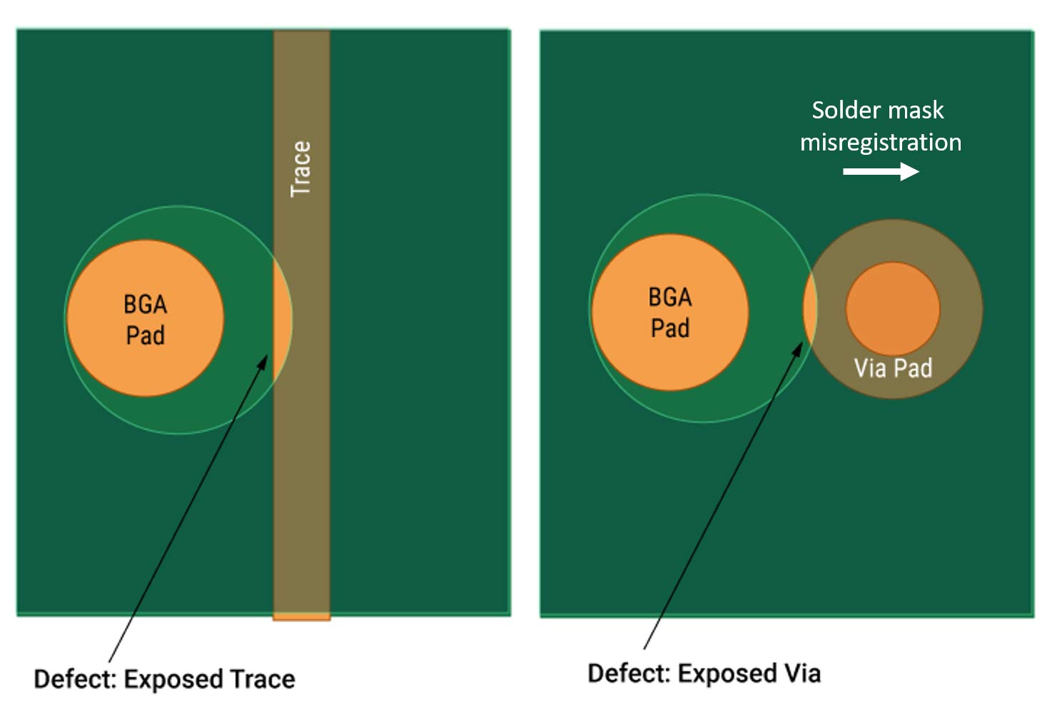
Solder mask registration
This is the alignment of the solder mask with reference to other board features, such as solder pads. Poor registration may cause the solder mask to overlap the pads or leave part of it exposed.
| Parameter | Standard | Advanced | Micro |
|---|---|---|---|
| Solder mask registration | 0.002” | 0.001” | 0.001″ |
Solder mask relief or solder mask web
The area on the board’s surface that does not have or doesn’t need solder mask is called solder mask relief. These are typically found around SMT pads, through-hole pads, test points, and vias and are left as a margin of error during fabrication.
Silkscreen checks

The silkscreen is a layer of non-conductive ink traces used to recognize components, test points, parts of the circuit board, warning symbols, logos, and other identification marks.
Silkscreen to mask spacing
The silkscreen to mask spacing is a clearance that is used to prevent the silkscreen marking from being printed over pads or on the board surface when it is undesirable. Standard silkscreen to mask spacing is 4.5 mils.
Silkscreen to copper spacing
Silkscreen to copper spacing is described as the least air gap required between any two adjacent copper traces or features. Standard silkscreen to copper spacing is 6 mils.
Silkscreen to hole spacing and route spacing
Board designers must place silkscreen outlines within defined boundaries to prevent overlapping with the minimum hole spacing and profile spacing. While implementing silkscreen outlines, ensure it does not overlap the component body. Standard silkscreen to hole/route spacing is 8 mils.
Effective implementation of the DFM rules will optimize the manufacturing processes and reduce the overall board cost. For more on design for manufacturing standards, download our DFM Handbook.
Design for Manufacturing Handbook
11 Chapters - 96 Pages - 90 Minute ReadWhat's Inside:
- Annular rings: avoid drill breakouts
- Vias: optimize your design
- Trace width and space: follow the best practices
- Solder mask and silkscreen: get the must-knows


