Jump scoring or skip scoring, is a technique utilized during the V-scoring process to prevent the PCBs from fully detaching from the panel during fabrication.
This technique ensures stability and minimizes the risk of damage until the boards are ready for depanalization.
What is jump or skip scoring in PCBs?
V-scoring is a technique utilized in circuit board manufacturing to aid depanelization. The process involves scoring the panel with a series of V-shaped double-sided cuts to create weak areas along which the circuit boards can be easily depanelized.

The thin incisions do not penetrate entirely through the material and serve as perforations on the laminate. This allows for easy removal of boards post-assembly through simple flexing or using a cutting wheel.
When dealing with heavy components or thin laminates, it’s necessary to prevent the V-score from cutting through the PCB rails within an array.
The additional rails are crucial to avoid premature part separation during the assembly process. To have the additional rails, the blades must be raised above the laminate surface before reaching the panel’s end. This procedure is known as PCB jump scoring, as the blades effectively jump over specific array sections.
Jump scoring can be achieved by incorporating a ½ inch breakaway edge on both the leading and trailing edges of the PCB array. The V-groove should extend approximately halfway through these edges to ensure effective scoring.
Jump scoring may not be utilized in every PCB manufacturing process, but it is certainly a beneficial option.
Also, see PCB milling to learn how slots, cut-outs, cavities, and board outlines are formed during fabrication.
When is jump scoring required?
V grooves can impact the structural integrity of your circuit boards, causing the leading and trailing edges to sag during the wave-soldering process. This can lead to the array’s warpage. Adding jump scoring to the array’s leading and trailing edges helps to strengthen it.
- Implement jump scoring when the V-score could potentially damage critical components or areas of the board during depanelization. By strategically avoiding certain sections of the array, jump scoring minimizes the risk of damage.
- When heavy components or thin laminates are present in your PCBA, jump scoring helps maintain the structural integrity of the array. Without jump scoring, there’s a risk of parts detaching prematurely from the array before assembly completion.
- Printed circuit boards, particularly those with a length exceeding 12 inches along either the X or Y axis, may become vulnerable to weakening and breakage if scored too deeply.
- Adding heavy components to an array elevates the risk of panel breakage during various stages, such as handling, assembly, or even during transit. Use jump scores or tabs to overcome this challenge.
How skip scoring is performed on circuit boards
Step 1: Preparation
The panel, which contains multiple individual PCBs arranged in an array, is prepared for V-scoring. This involves ensuring that the panel is securely held in place and aligned properly for the scoring process.
Step 2: Programming
The V-scoring equipment is programmed to execute the scoring process according to your requirements. This includes determining the locations of the V-scores and configuring any jump-scoring parameters.
Step 3: Scoring
The V-scoring machine operates by moving a set of blades (top and bottom) across the panel in straight lines, cutting partially through the material but leaving small uncut sections (jumpers) along the scored lines where needed.
Alternatively, in some older equipment, the blades may remain stationary as the panel is moved across them.
Step 4: Jump scoring
During the scoring process, when the blades approach areas where jump scoring is required (such as rails or areas with heavy components), they are lifted off the laminate surface to avoid cutting through certain sections of the array. This ensures that the array’s structural integrity is maintained.
Learn about the essential PCB mechanical processes that shape and prepare circuit boards for assembly.
Importance of indicating jump scoring in the fab drawing
When creating part drawings, it’s crucial to clearly communicate the intended manufacturing processes and requirements. Simply drawing V-score lines without explicitly stating the need for a jump V-score can lead to confusion or misinterpretation by those responsible for manufacturing.
Sometimes, the PCB array panelization is designed before considering V-scoring. In such cases, there’s a risk that the score might not be appropriately placed within the rails, leading to parts being jump-scored unintentionally.
On the other hand, if V-score lines are drawn that pass through the parts but not through the rails, without mentioning the jump V-score, it might result in unexpected outcomes during manufacturing.
Failure to call out the jump score on the drawing means that manufacturers may miss the intended V-score requirement. This could result in the V-score going all the way through the panel, causing damage to the parts and potentially leading to incorrect production.
Hence, when the V-score is not intended to cross the entire panel, it can be called out on the fab drawing as a table score, and the locations can be noted using arrows, leaders, notes, and other methods.
To make sure your design is manufacturable the first time, download our e-book.

Design for Manufacturing Handbook
11 Chapters - 96 Pages - 90 Minute ReadWhat's Inside:
- Annular rings: avoid drill breakouts
- Vias: optimize your design
- Trace width and space: follow the best practices
- Solder mask and silkscreen: get the must-knows
Download Now
Challenges during the skip score process
Premature blade elevation
Premature blade elevation risks thinner V-score depths and complicates depanelization. You can avoid this by accurately defining the jump score parameters in your fab drawing.
Inaccurate blade movement
While the scoring equipment is still in operation, the blade will rise from the panel, causing slight scoring in the waste area. This results in a shallower score and poses challenges during depanelization.
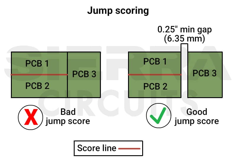
Further, it’s not possible to halt the scoring process precisely at the endpoint of a score-line. To ensure a full score, the scoring blade needs to travel beyond the endpoint before stopping. A minimum gap of 0.25 inch (6.35 mm) must be maintained between the designated stop score location and any area not meant to be scored.
We ensure precise programming and calibration of our V-score equipment to ensure accurate blade elevation.
To learn more about our expertise in circuit board fabrication, see our PCB manufacturing services.
Precise jump scoring relies on advanced V-score equipment to program blade elevation for accurate lifting during panel processing. However, the limitations and costs associated with this method make the use of tab routing preferable over jump scoring.
With the increasing number of surface components on PCBs, jump scoring has become more common. To avoid assembly errors, you need to depict these requirements accurately on drawings.


