Speak to an Account Manager
![]() +1 (800) 763-7503
+1 (800) 763-7503
Tools for Designers:
Via Thermal Resistance Calculator
Sierra Circuits Via Thermal Resistance Calculator computes the required number of thermal vias you can include in a via arrangement connecting a thermal pad. This calculator also optimizes the drill diameter and spacing between two vias for a given number of thermal vias.
Try This New ToolEffective heat transfer mechanisms in PCBs are crucial to enhancing their performance and reliability. They also aid in lowering noise levels and overall product costs. To provide a systematic thermal route from the chip (IC) to the heatsink, plated through-hole vias are implemented. These vertically drilled vias, known as thermal vias, typically connect all the layers of a board. Understanding the thermal resistance of these through-holes will help in determining their heat dissipation capacities.
Sierra Circuits’ Via Thermal Resistance Calculator computes the required number of thermal vias you can include in a via arrangement connecting a thermal pad. This calculator also optimizes the drill diameter and spacing between two vias for a given number of thermal vias.
Features of the tool
- Supports two types of via pattern (via pattern 1 and via pattern 2)
- Provides a list of commonly used conductive and non-conductive epoxy via fills along with their thermal characteristics (Tg, CTE, and k)
- Supports multiple units(mm of via dimensions and plating thickness
- Determines the thermal resistance of via/vias by optimizing drill diameter and via-to-via spacing
- Input units can be changed
How to use the Via Thermal Resistance Calculator
The input parameters for this tool are:
- Length of the thermal pad (l)
- Width of the thermal pad (w)
- Thermal conductivity of copper
- Thermal conductivity of the filler
- Via height
- Plating thickness
The output parameters:
- Thermal resistance of the single via
- Thermal resistance for the total number of vias
Calculating drill diameter
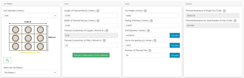
First, choose the desired via pattern from the drop-down.
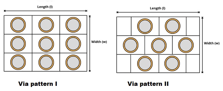
Via patterns
Now, input all the default parameters along with via to via spacing and the number of thermal vias and hit calculate beside the drill diameter field. The tool will display the optimum drill diameter.
How to compute via to via spacing
Enter the values of all the default input parameters (length of the thermal pad, width of the thermal pad, thermal conductivity of copper, thermal conductivity of the filler, via height, and plating thickness), drill diameter, and the number of thermal vias. Click on calculate adjacent to the via to via spacing section. The suitable spacing values for your thermal vias will be displayed.
Identifying the number of thermal vias
Here, you need to enter the values of all the default input parameters (length of the thermal pad, width of the thermal pad, thermal conductivity of copper, thermal conductivity of the filler, via height, and plating thickness), via to via spacing, and drill diameter. Next, hit calculate alongside the number of thermal vias section.
Sierra Circuits’ Via Thermal Resistance Calculator is an advanced PCB design tool that expedites the process of designing thermal vias. Using this application, you can quickly identify the thermal resistance of a single or a combination of vias. You can also calculate the accurate drill diameter, via to via spacing, and the thermal vias that can go into a thermal pad.
Watch the tool demo:

Sierra Circuits has developed easy-to-use tools for PCB designers and electrical engineers at every stage of circuit board development.


Fabrication, Procurement, & Assembly. PCBs fully assembled in as fast as 5 days.
- Bundled together in an entirely-online process
- Reviewed and tested by Engineers
- DFA & DFM Checks on every order
- Shipped from Silicon Valley in as fast as 5 days

Fabrication. Procurement & Assembly optional. Flexible and transparent for advanced creators.
- Rigid PCBs, built to IPC-6012 Class 2 Specs
- 2 mil (0.002″) trace / space
- DFM Checks on every order
- 24-hour turn-times available

Complex technology, with a dedicated CAM Engineer. Stack-up assistance included.
- Complex PCB requirements
- Mil-Spec & Class 3 with HDI Features
- Blind & Buried Vias
- Flex & Rigid-Flex boards