Most PCB designers create fabrication and assembly files to go along with their board designs. The problem is that sometimes these designers don’t know everything that a contract manufacturer needs in those drawings to successfully build the board. Creating a simple drawing using PCB design CAD tools is pretty easy, but without all of the necessary manufacturing data, a simple drawing won’t be enough. That is the only reason most of the CMs take a lot of time to get a hold of the missing details.
What do you mean by design deliverables for manufacturing and assembly?
PCB fabrication, assembly, and test require a set of industry-specific information in the form of schematic drawings, stack-up drawings, BOM, etc. Manufacturers also customize these deliverables as per their capabilities and customer requirements.
Types of fabrication and assembly files required for manufacturing
Fabrication drawing
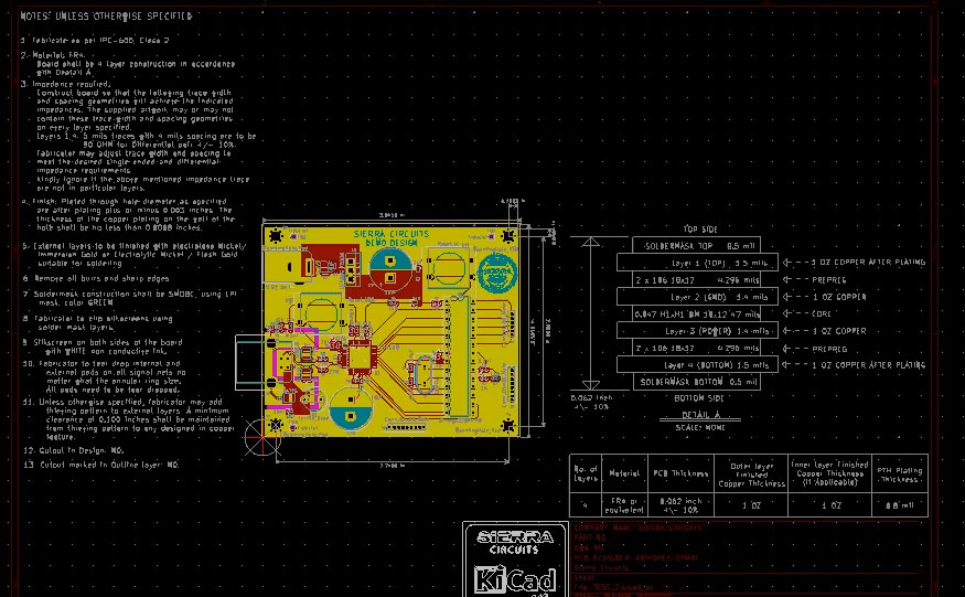
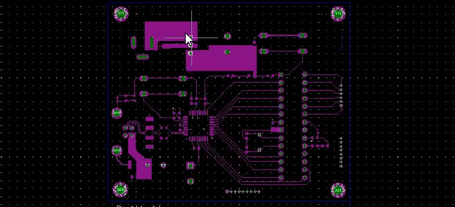
The fabrication drawing includes all of the drilled holes in the board and is usually auto-generated by the CAD system. Include that dimension features such as the board outline and mounting holes, and specific notes that mention the details of the board’s construction.
The following points should also be included:
- A complete stack-up view specifying layer dimensions and board materials. Some of the detailed board materials are often included in the fab drawing notes, as well.
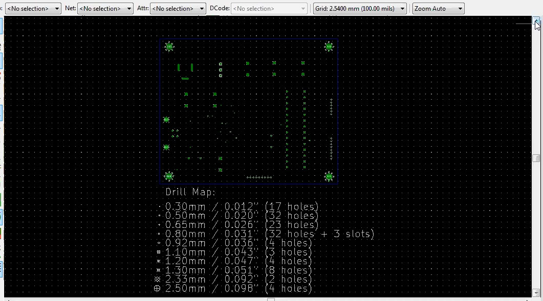
- Complete drill location information with different drill symbols for each size. There should also be a separate drill chart that associates the finished hole size with the symbol.
- Non-standard board features, such as slots or cut-outs, must be fully dimensioned. These often aren’t included in the NC drill file and should be included in the drawing.
- Processing requirements, such as silkscreen color, solder mask color or controlled impedance trace routing details for each signal layer, should be included in the drawing notes.
- Manufacturing class (class 2 or 3) based on the application requirement.
Assembly drawing
Like the fabrication drawing, the assembly drawing is also typically auto-generated from the PCB design CAD tools. This drawing shows all of the components on the board in their assembled locations, along with their corresponding reference designators for identification. Designers also include some notes to instruct the manufacturer about how the board is to be assembled. Depending on the complexity of the board though, there may be a lot more that needs to be included. Consider the following while creating an assembly drawing:
- Critical components, like connectors or heat sinks that need specialized mounting instructions, should be mentioned in the assembly notes on the drawing.
- Additional hardware that is to be mounted onto the board, such as stiffener bars, handles, or ejectors, should be shown with their specific instructions included in the drawing notes.
- Critical areas of assembly should have an exploded view or detail shown that is enlarged and pulled away from the rest of the board image.
- The location of assembly stickers and labels should also be shown on the drawing.
Bill of materials (BOM)
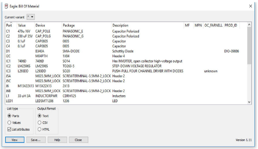
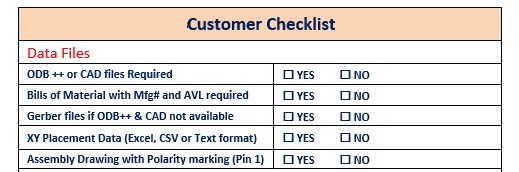
A bill of materials for an electronic product lists all the components used to build it. The example below shows a customer checklist and we can see that BOM is one of the many important documents submitted by the customer to a PCB manufacturer.
Additionally, the BOM generator will report exactly what is built into the design database. If there are part errors, they will get reported in the BOM. Here are some examples of items one should double-check to ensure the BOM file is complete and correct:
Description mismatch: When the description of the part in the BOM doesn’t match the description of the part numbers, it slows PCB assembly until the BOM descriptions can be verified.
Missing reference designators: Without reference designators on listed parts in the BOM, the manufacturer doesn’t know which parts get installed to which footprint on the board.
Incorrect or partial manufacturing part numbers: Sometimes, trailing dash numbers are omitted on the BOM, or the part number is incorrect. This will force the PCB manufacturer to delay the build until they can check with you.
Incomplete information: In some cases, entire parts may be left out of the BOM. This can easily happen if the PCB designer forgets to update the BOM after a design change has gone through. This may not even show up in the assembly process until it is clear that there are missing components on the board.
IPC netlist
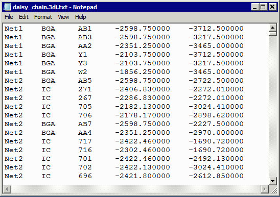
This data file often doesn’t get sent to the CM because it isn’t a typical Gerber, drill, or BOM file. However, the CM will use this netlist to develop the test fixtures and procedures, as well as to identify board fabrication details that need special attention.
Gerber files
Gerber files are generated for each of the layers of a PCB. The manufacturer produces as many as 30 or more layer files to define different aspects of manufacturing.
List of gerber files for board manufacturing
- Aperture definitions
- TOP- Top layer – This defines the top copper layer, traces, and pads
- SMT – Solder Mask Top – Defines the area where soldermask should appear on the top layer
- SPT – Solder Paste Top – Defines the solder paste applied to solder the components on the top layer
- BOT – Bottom layer
- SMB – Solder Mask Bottom
- SPB – Solder Paste Bottom
- SST – Silkscreen top – Defines the labels on the top layer of the components
- SSB – Silkscreen bottom – Defines the labels on the bottom layer of the components
- AST – Assembly top – Assembly instructions of the top layer
- ASB – Assembly Bottom – Assembly instructions of the bottom layer
- FAB – Gives details of drills, stack-up, cutouts, and fabrication instructions such
as the class of fabrication (class 2, class 3).
NC drill files
A drill file is a secondary file sent to the manufacturer with the Gerber file. The drill file refers to the position, size, and the number of holes in the desired PCB. The NC drill file can be used to correctly determine where all the drill holes are located on the board and the size they require. The number of files created for the drill varies depending on the complexity of the PCB wiring. Drills can be of different types: through-holes, blind vias, and buried vias.
Pick and place files
The main purpose of pick and place data is to hold information about the position and orientation of all surface mount devices on a circuit board design. So pick and place files contain data such as:
- Reference designators
- XY locations of the component in the board
- Orientation of the component in degree (45°, 90°, etc.)
- Component packages – Part number, Part value, etc.
- Placement on either the top or bottom side of the board
ODB++
ODB++ is an intelligent format. This file or directory contains all the information required to define a circuit board layer.
This file format offers a stable framework for the required data. An ODB++ file allows the designer to combine all the required data and perform the necessary checks for manufacturability and reliability.
Read PCB file formats to choose the right files to communicate your design intent to manufacturers.
List of other fabrication files
Stack-up drawing
Designers can draw a stack-up describing details such as the thickness of each layer, the thickness of the top and bottom solder mask. It includes information such as finished PCB thickness, core thickness, prepreg thickness, copper thickness for PTHs and vias, and copper cladding thickness.
Schematics drawings
3D files
Some of the ECAD tools can generate step files from the design files. Step files give a 3d view of the design. One can visually check the placement of the components. This is especially useful to check whether the direction of the connectors is correct.
Special assembly instructions
Some electronic products require components to be soldered in a specific way such as through-hole components, say transistors which need to be soldered at specific heights. Also, cables need to be of a certain length and have to be soldered in a certain way. Such stringent instructions need to be documented and provided with the fabrication files.
By including these board fabrication and assembly details in fab drawings, circuit board manufacturing and assembly rate can be improved considerably, resulting in a quicker delivery time.

PCB Design for Assembly Handbook
6 Chapters - 50 Pages - 70 Minute ReadWhat's Inside:
- Recommended layout for components
- Common PCB assembly defects
- Factors that impact the cost of the PCB assembly, including:
- Component packages
- Board assembly volumes
Download Now


