PCB assembly notes provide project-specific instructions that help manufacturers assemble, inspect, and verify the circuit board according to the design requirements.
In this article, you’ll learn about the documents required for PCBAs and what you should include in your assembly notes.
Highlights:
- Assembly notes communicate designer requirements to the contract manufacturer (CM).
- IPC standards such as IPC-CM-770, IPC-A-610, J-STD-001, J-STD-003, and IPC-1066 are typically referenced in instruction documents.
- The documentation also includes drawings, schematics, and the bill of materials (BOM).
What documents does your PCB assembly house require?
The following is the list of documents required for the circuit board assembly:
- Assembly drawing
- Assembly notes
- Schematic diagram
- Bill of materials
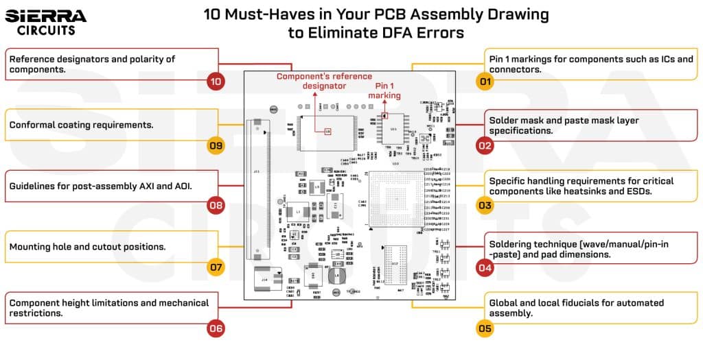
What is an assembly drawing?
It displays all the components on the board in their assembled locations, along with their corresponding reference designators for identification.


Here’s what you need to include in your drawing to avoid DFA errors and ensure seamless prototype production.
What are PCB assembly notes?
They are a formal set of written instructions and requirements included on the assembly drawing or in the fabrication package. They define how the board must be assembled, inspected, and handled to meet the design intent, and they become part of the contract with the manufacturer.
For more, download the PCB Fab and Assembly Notes for Designers.

PCB Fab and Assembly Notes for Designers
8 Chapters - 72 Pages - 70 Minute ReadWhat's Inside:
- Guidance on how to write comprehensive fab documentation
- Advanced fabrication notes for flex, rigid-flex, and hybrid stack-ups
- Difference between fabrication and assembly notes
- Assembly documentation essentials: BOM, X-Y data, and drawings
Download Now
What should you include in your printed board assembly notes?
Specify the key instructions and constraints needed to assemble the board correctly. The notes typically communicate board orientation, reference designators, component mounting requirements, soldering instructions, and any special component placement methods. Let’s look at them in detail.
Primary and secondary board side identification
All circuit boards have their sides designated as the primary (top side) and the secondary side (bottom side) based on the design needs. You should use the same primary side designation in both the board fabrication and the PCB assembly drawing.
The pictorial representation should portray the primary side of the board as the top view in the drawing. In cases where components are present on both sides (primary and secondary), an additional view displaying the secondary side should be added to the layout.
Reference designators

The designators are typically printed onto the board. Although stakeholders might sometimes miss the printed reference alphanumeric markings on the PCB. In some cases, there might not be sufficient space to print some or all markings. In such cases, the notes should clearly communicate the required markings that cannot fit on the board.
A good assembly drawing has the unique advantage of scalability, which enables designers to show component designators adequately. Such designators should be legible and placed within the component outline to guide component placement and inspection.
Example: Components are identified by checking the reference designators in the bill of materials against those on the face of the drawing. Reference designators are used for reference purposes only and may not appear on the board or part.
Component mounting requirements
IPC-CM-770 guidelines for printed circuit board component mounting specify effective methods of component mounting. Including this specification in the drawing helps customers and manufacturers, or designers and fabricators, communicate the component mounting requirements clearly.
In addition, IPC-A-610 defines the acceptance criteria for every assembly operation and serves as the manufacturing acceptance specification, regardless of the mounting method used.
For boards with manually mounted components, include the component height restrictions in the drawing. When necessary, also specify the required clearances from adjacent components.
Example:
- PCB component mounting shall conform to IPC-CM-770.
- Acceptability of this PCBA shall conform to IPC-A-610 class 2.
Soldering instructions
J-STD-001 is the joint global industry standard for electrical and electronics assembly soldering. It details the materials, techniques, and verification needs for all features for creating high-quality solder joints. J-STD-003 defines the standard for solderability testing and includes defect definitions along with their diagrams.
Designers can reference these two specifications together in notes to verify the quality of solder interconnections.
Example: Solder per J-STD-001 and J-STD-003.
Specialized assembly methods
The notes document any specialized instructions, such as lead-free requirements, environmental specifications, and marking requirements. For military and space applications, designers specify the applicable environmental and lead-free requirements in the assembly notes. They may also reference IPC-1066 to define the required marking methods for these assemblies.
IPC-1066 does not apply if:
- Lead is used as an alloying element in:
- Steel: 0.35%
- Aluminum: 0.4%
- Copper: 0.4%
- Lead is present in electronic ceramic parts used in piezoelectric devices.
The circuit board shall satisfy the specified environmental requirements. Apply the appropriate solder material category markings in accordance with IPC-1066.
For more details, book a meeting to talk to a PCB expert or call us at +1(800) 763-7503.
What aspects of PCBA does IPC-A-610 cover?
The standard sets the acceptability criteria for assembled circuit boards. It defines the requirements for a PCBA, including component mounting (THT and SMT), soldering, handling, markings, solder mask, and other workmanship requirements.
IPC-A-610 categorizes PCB assemblies into three classes:
- Class 1: Manufacturers use this class for non-critical products that do not require strict adherence to IPC guidelines, such as those used in toys.
- Class 2: This class applies to products that are not mission-critical but require a higher level of operational reliability.
- Class 3: Here, the products manufactured need to adhere strictly to all the IPC guidelines.
Sierra Circuits fabricates and assembles high-performance boards compliant with IPC, ISO, mil-spec, and ITAR standards.
To learn more, see PCB manufacturing capabilities.
Precise printed board assembly notes streamline the manufacturing process and help manufacturers build your boards according to your design requirements.
See our FAQ on PCB assembly for more information.


