BGA assembly is necessary to implement complex and small-size chips in PCB designs to match technological advancements. This increases the packaging I/O density. Ball grid array is a high-density and low-cost packaging method.
What is ball grid array (BGA) assembly?

BGA assembly is a process of mounting ball grid arrays onto a PCB using the solder reflow process. They are surface-mount components that use arrays of solder balls to make electrical interconnections. These solder balls melt and establish interconnection when the board passes through the solder reflow oven.
What are the advantages of a BGA assembly?
- Improves both electrical and thermal performance while making efficient use of space.
- Reduces the overall thickness of the board.
- Minimizes the chances of PCB damage since BGA leads are made from solid solder balls, consequently reducing maintenance and repair times.
- Suitable for miniature packages with high pin count.
- Offers improved solderability, resulting in a speedy assembly procedure.
- Dissipates heat quickly due to low thermal resistance.

HDI PCB Design Guide
5 Chapters - 52 Pages - 60 Minute ReadWhat's Inside:
- Planning your stack-up and microvia structure
- Choosing the right materials
- Signal integrity and controlled impedance in HDI
- Manufacturing considerations for higher yields
Download Now
PCB design considerations for BGA
- Use dog bone with the boulevard routing method when the pitch allows it (greater than 0.65 mm).
- Separate each via from its pad with a predefined short trace covered with a solder mask. Ensure there is no mask clearance for the vias under the BGA and the non-via-in-pad vias are covered with solder mask.
- Use the via-in-pad technique for smaller pitches as it accommodates tighter component pitch sizes (like 0.5 mm) and reduces the overall size of the PCB.
- The pad matrix on which a ball grid array will be installed may include through-hole and blind vias, but those vias must be filled and planarized. Otherwise, it will lead to solder joint issues.
- Use circular stencil aperture for BGA packages. A round aperture shape allows uniform overprinting on a round pad. Square corners can result in the non-uniform deposition of solder paste so they should be avoided. Based on the aperture area ratio, stencil material, and aperture diameter, the stencil aperture can vary between 100 microns (0.1 mm) to 150 microns (0.15 mm).
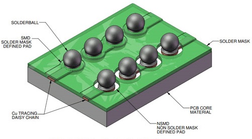
- Non-solder-mask-defined (NSMD) pads are generally chosen for 0.5 mm or greater pitches.
- For ultra-fine pitch BGAs having a pitch of 0.5 mm or below, it is preferred to use via-in-pad technology since a dog-bone type of fan-out cannot be performed.
- For ball grid array packages, solder ball pitch generally remains at 50 mils or below. To fulfill the technology requirement used in the PCB fabrication process, the spacing between the through-hole and copper should be at least 8 mils and the spacing between traces and pad edge can be reduced to 3 mils. Therefore, keep the pad size of BGA chips between 14 and 22 mils and trace width between solder balls between 3 mils to 5 mils.
- For array packages like BGAs, in which a solder joint is formed on the bottom side, a no-clean paste is used to avoid further cleaning in the later stages. When placing ball grid arrays, apply optimum placement force because excessive force will squeeze the solder paste out, resulting in solder joint shorts.
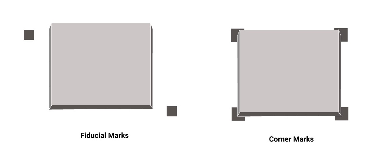
- Since BGA packages cannot be inspected by the naked eye, fiducial marks should be compatible with assembly inspection, manual assembly, and replacement after rework. Always place either two fiducial marks at opposite corners of a ball grid array component or two corner marks, as depicted in the following figure.
- Use NSMD style landing pad in BGA packages. The NSMD pads are those in which the pad is not covered by a solder mask.
- The number of layers on a PCB that contains a BGA is determined by a simple formula.
Number of layers = [Total numbers of solder balls in a BGA × 0.6/ (Number of routing channels × Routes per channel)]
- When placing BGA components on both sides of the PCB, do not place BGAs directly opposite to each other. The temperature cycle board-level reliability (BLR) reduces if the board is designed with overlapping BGAs. Hence, always maintain some offset when placing BGAs on both sides of the board.
BGA pads having a pitch of 0.5 mm to 0.8 mm that use blind vias should have a drilled via diameter less than or equal to 0.004” (0.1016 mm) and an aspect ratio less than or equal to 0.75:1.
All vias should be tented, filled, and/or capped, especially under ball grid array packages.
How to ensure good soldering in BGA assembly?
- Adequate heat should be applied so that all the balls in the grid melt to realize a strong bond for every BGA solder joint.
- The surface tension of the molten balls locks the BGA package in place until the solder cools and solidifies. A temperature-controlled soldering process is essential for establishing quality solder joints. This practice also prevents solder balls from short-circuiting each other.
- The configuration of the solder alloy and soldering temperature is chosen precisely so that the solder doesn’t completely melt but stays semi-liquid. It allows each ball to stay separate from its neighboring balls. Always stick to the reflow temperature profile given by your component manufacturer.
How to check solder joint quality?
Optical techniques are not suitable for inspecting ball grid arrays since the solder joints are hidden from sight under the BGA components. Additionally, electrical tests aren’t very reliable since they reveal the electrical conductivity of the BGA at a particular instant. Such tests don’t predict if the solder will last long or not. The solder joint may in fact fail after some time.
Unlike electrical tests, X-rays are used to inspect the BGA solder joint. It helps to look through the solder joint beneath the BGAs. Due to this advantage, the automated X-ray inspection (AXI) technique is widely used to perform BGA inspection.


