


Contents
A pad in PCBs is the copper area where electronic components are soldered to the board. They provide both mechanical support and electrical connectivity, forming the interface between component leads and the traces.
Proper pad sizing and geometry are critical for reliable solder joints, manufacturability, and long-term performance.
In this blog, you will learn how different PCB pad types are designed, how pad geometry affects manufacturability and reliability, and how IPC standards guide accurate pad sizing for modern PCB assemblies.
Highlights:
- PCB pads form the foundation of reliable electrical and mechanical connections.
- Surface-mount and through-hole pads differ significantly in structure and application.
- BGA pad design directly impacts solder joint reliability and routing density.
- Via-in-pad is essential for compact HDI designs, but requires controlled fabrication.
- Manual pad design errors often lead to assembly and reliability failures.
- IPC standards provide consistent rules for pad sizing and manufacturability.
What is a pad in PCB design?
A pad is the exposed region of metal on a circuit board to which the component lead is soldered. Multiple pads are used in conjunction to generate the component footprint or land pattern on the printed board. The two types of pads available are through-hole and surface-mount pads.
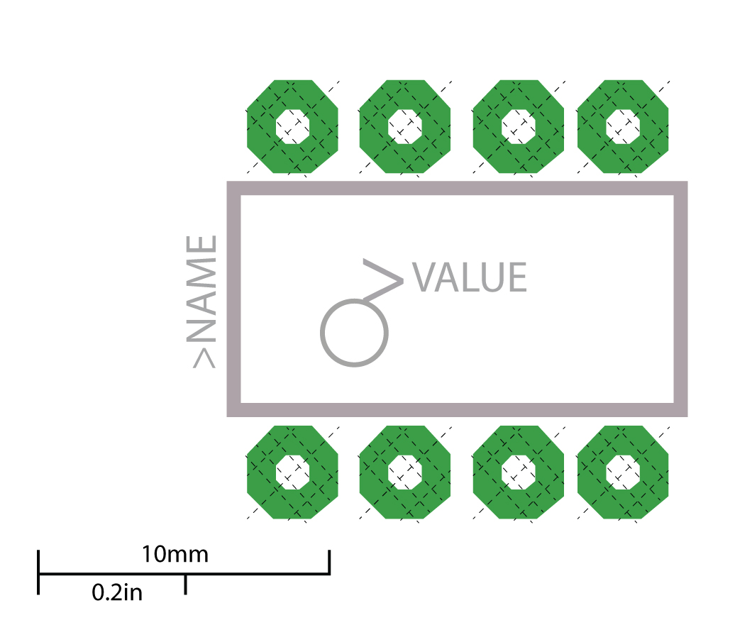
What is a surface-mount pad?
An SMT pad is a copper feature designed to solder an SMD directly onto the board surface. Their geometry, solder mask definition, and paste coverage strongly influence solder joint formation, component alignment, and reflow quality, especially for fine-pitch and high-density assemblies.
What are the special features of the BGA pad?
BGA pads are designed to ensure reliable solder ball attachment, uniform joint formation, and effective signal and thermal performance in high-density PCB designs. Proper pad design is critical to ensure the manufacturability of BGA components.
There are basically two types of BGA pads: the solder mask-defined pad (SMD) and the non-solder mask-defined pad (NSMD). Read the SMD pad vs NSMD pad to know more.
Solder mask defined (SMD) BGA pads
SMD pads are defined by the solder mask apertures applied to the BGA pads. These pads have the solder mask aperture such that the mask opening is smaller than the diameter of the pad they cover. This is done to shrink the copper pad size that the part will be soldered to.
The image shows how the solder mask has been specified to cover a part of the copper pad underneath. This can lead to two advantages – firstly, the overlapping mask helps prevent the pads from lifting off the board because of mechanical or thermal stress.
The second advantage is that the opening in the mask will create a channel for every ball on the BGA to align with while the part moves through the soldering process.
The copper layer of an SMD BGA pad conventionally has a diameter equal to the pad on the BGA. To generate the SMD overlay, a reduction of 20% is traditionally used.
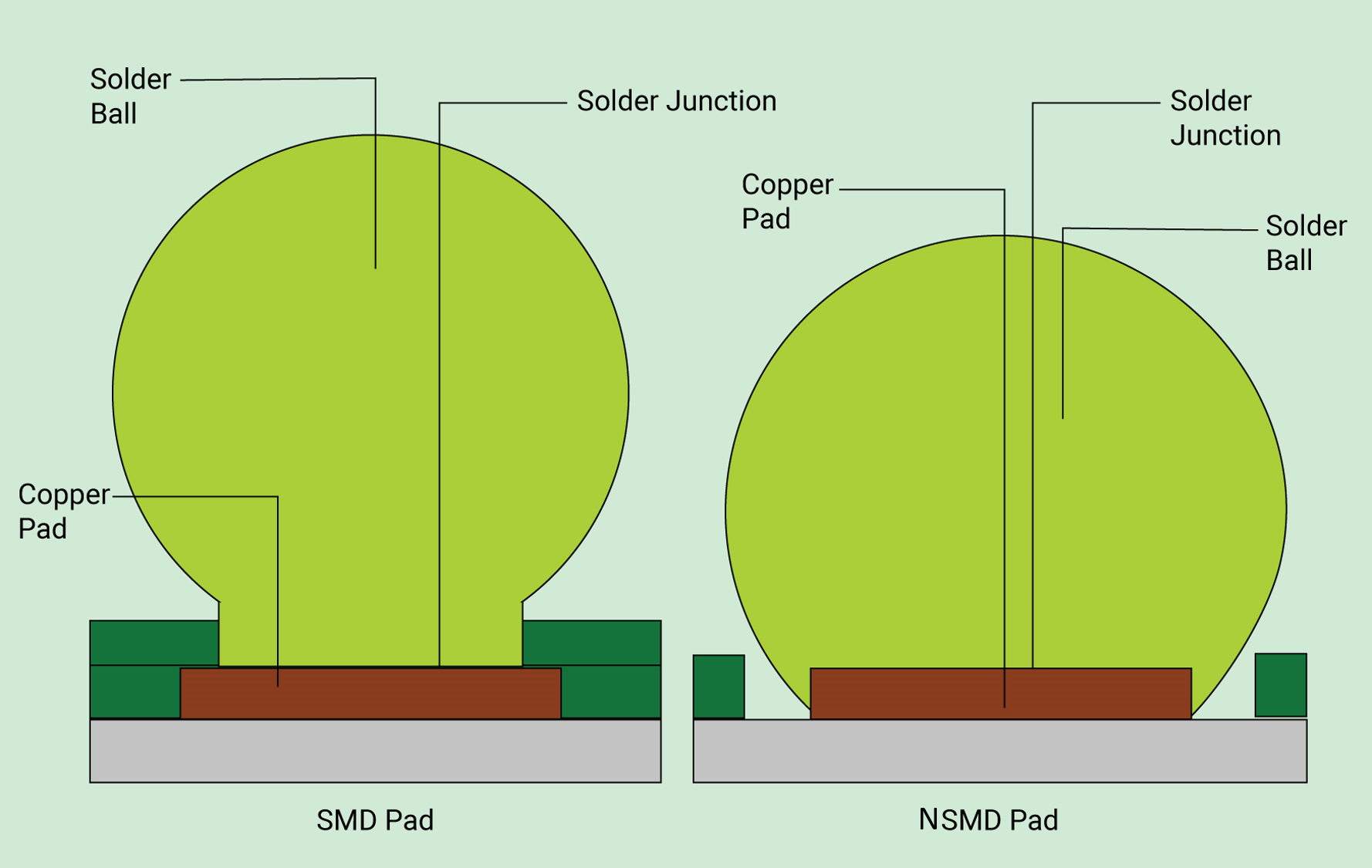
Non-solder mask defined BGA pads (NSMD)
NSMD pads vary from SMD pads in that the solder mask is defined not contact the copper pad. The mask is instead created such that a gap is generated between the pad edge and the solder mask.

Here, the copper pad size is defined by the copper pad diameter instead of the mask layer.
NSMD pads can be smaller than the diameter of the solder ball, and this reduction in pad size is 20% of the ball diameter. This approach leaves more room between adjacent pads, enabling easier trace routing, and is used for high-density and fine-pitch BGA chips.
One disadvantage of NSMD pads is their high susceptibility to delamination due to thermal and mechanical stresses. However, NSMD pad delamination can be prevented when standard manufacturing and handling practices are followed.
What is a through-hole pad?
A through-hole pad is a plated copper area surrounding a drilled hole that provides a strong mechanical and electrical connection for components with leads passing through the PCB. There are two types:
Plated through-hole (PTH)
PTH refers to a pad with a through-hole. The hole wall will be plated with copper and sometimes with solder or another protective plating. The hole plating is done using the process of electrolysis.
The plating provides for an electrical connection between the different layers of the board. In castellated boards, the holes are drilled on the edges of the board. These semi-holes will be plated to make connections with another sub-module.
Non-plated through-hole
NPTH refers to a pad without plating in the hole. This pad is mostly used for single-sided boards, or these holes are used for mounting the PCB in an enclosure, and screws are mounted through these holes.
Conventionally, unplated holes will have an area around the hole that is clear of any copper (similar to board edge clearance). This is done to prevent shorts between copper layers and parts that are to be placed.
The different parts of a through-hole pad are typically called a pad stack, which consists of:
- Top pad
- Bottom pad
- Inner pad
- Drill
- Annular ring
- Pin number
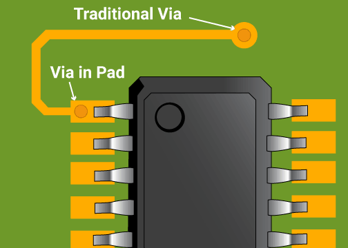
Can you place a via on a pad?
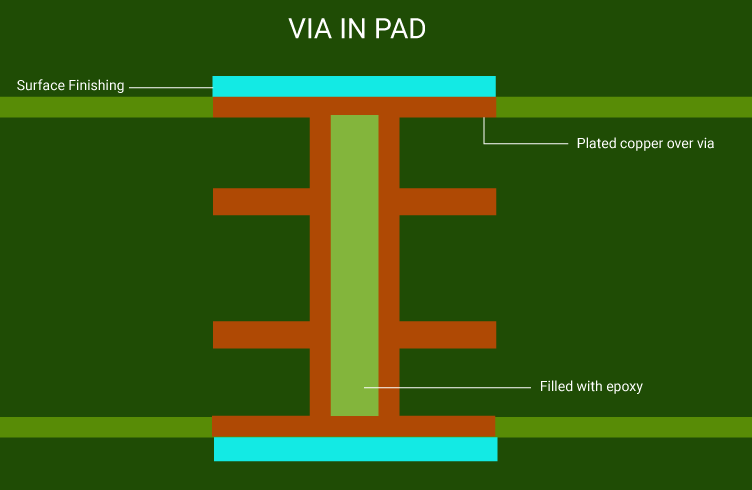
Yes, via-in-pad technology allows a via to be placed directly within a component pad to save routing space. This approach is widely used in HDI designs and fine-pitch BGAs but requires via filling and planarization for reliable assembly.
Via-in-pads are commonly used for BGA components with pitches of 0.5 mm or less.

High-Speed PCB Design Guide
8 Chapters - 115 Pages - 150 Minute ReadWhat's Inside:
- Explanations of signal integrity issues
- Understanding transmission lines and controlled impedance
- Selection process of high-speed PCB materials
- High-speed layout guidelines
Download Now
What is a bond pad?
A bond pad serves the purpose of connecting the circuit on a die to the pin on a packaged chip. One side of a gold wire will connect to the bonding pad, while the other side will connect to the package.
The bonding pad is made from all metal layers stacked on top of each other and connected through the vias. This allows connection from the chip core to the pad.
The die will also require an insulator or passivation layer on the complete chip to protect the core from environmental contamination. The bonding pads are required to be accessible for connection to the chip package and hence can not be wrapped by the insulator layer.
The glass layer is used to inform the manufacturer where the openings need to be for bonding. Also read, PCB Via Design Using Altium Designer
What is via plugging in PCB?
Via plugging is a technique used to completely fill vias with resin or closed with a solder mask. This process differs from via tenting in that resin or solder mask does not fill the via hole, but just offers a covering.


Via plugging is implemented as a preventive measure to secure the vias against the undesirable flow of solder during the soldering process. When a via is not plugged or tented during a soldering process, the solder can flow into the via from the pads and create unwanted solder joints.
Via plugging can be implemented using a conductive or non-conductive material. Conductive filling for vias helps conduct current from one side of the board to another. The disadvantage of using conductive filling is the difference in coefficient of thermal expansion (CTE) between the surrounding laminate and the conductive fill.
While the PCB is in operation, the conductive material will heat at a faster rate than the surrounding laminate, expand, and cause fractures. This is between the via wall and the contact pad under consideration.
Via holes that are filled with non-conductive materials will be able to work as a normal via, but will not have the ability to carry high currents, such as the conductive-filled vias.

5 common errors in manual pad design
These days, automation is used to eliminate the manual design of pads. It involves drawing the required pad shapes using design software tools. This can be mapped using datasheets and formulas for generic pad shapes and sizes.
The manual process is prone to errors as fabricator specifications don’t always stick to the same formulas as in automated processes. It results in wrong pad shapes and sizes, leading to undesirable results such as:
1. Through-hole breakout
Through-hole pads need a solid annular ring for solderability. The annular ring is the metal between the outer perimeter of the pad and the hole wall. An annular ring’s size specification needs to be large enough to compensate for the drill to wander from the center of the hole.
When the pad is too small, it might lead to a breakout, resulting in broken, incomplete circuits or improper soldering.
2. Insufficient solder joints
SMT components with pads that are too small might not get a proper solder fillet during the soldering process. The lack of a good fillet can lead to a solder joint that is weak and can break.
3. Floating parts
Here, SMT components that are mounted on pads that are too large could float out of position during the solder reflow process. This might lead to shorts between circuits.
4. Tombstoning parts
SMT components with two leads that are smaller, such as resistors and capacitors, can have issues when the pads are not of the same size. This defect, where one pad will heat faster than the other, is called tombstoning, as the component will pull up from the other pad, looking like a tombstone.
To learn more about tombstoning, read 8 common errors in surface mount technology (SMT).
5. Shorts to other metal
Pads that are smaller than the requirement might permit surface traces close to the components soldered onto them, leading to shorting possibilities. Pads larger than the requirement could hamper routing between the pads, turning routing into a challenge.
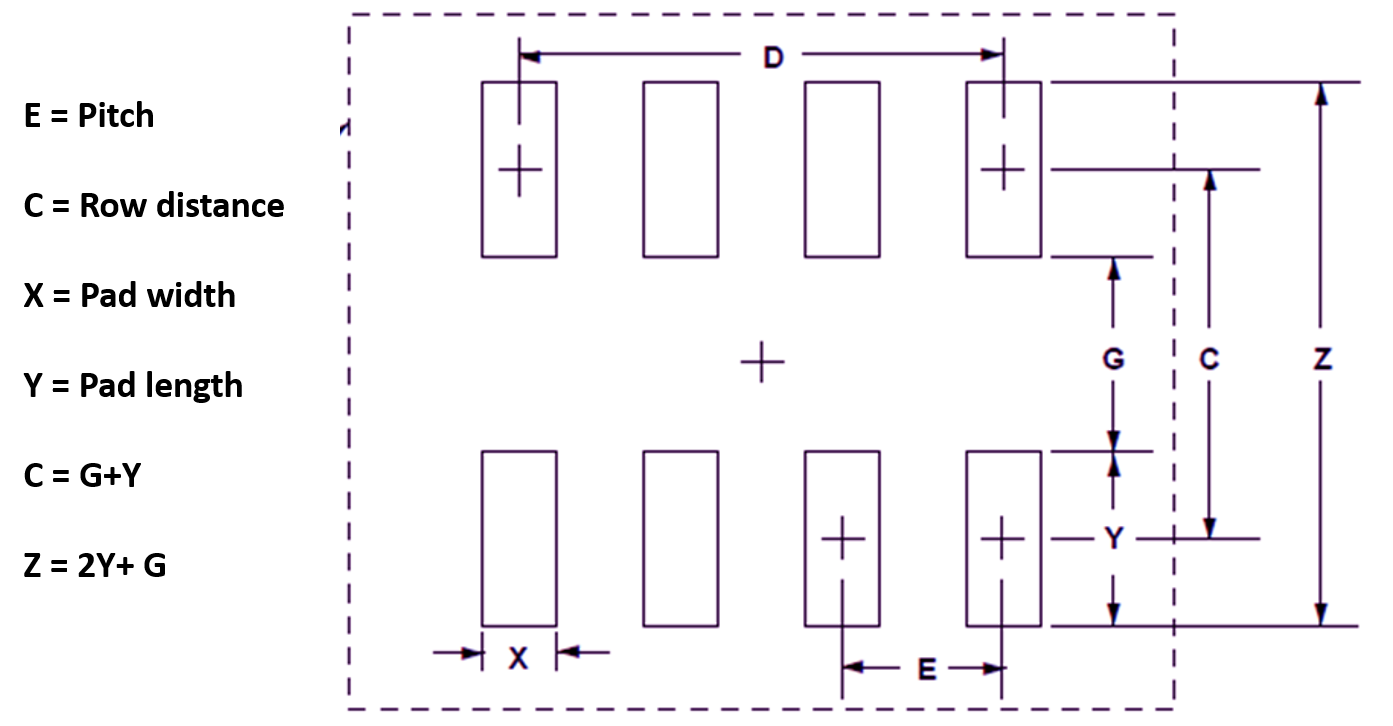
What are the different elements in a pad stack?
Pad stack elements typically include the copper pad, drill hole, plating, solder mask opening, and optional surface finish that together define the pad’s electrical and mechanical behavior.
The most common type of hole in a PCB is the plated through-hole. A pad stack includes all the features of a drilled hole that can be a plated, non-plated, buried, or blind hole.
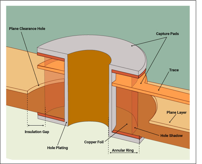
The image above displays the critical aspects of a drilled hole that are defined as follows:
- Via: This is any plated through-hole that is utilized to either connect a signal from the board surface to an internal layer or to change layers.
- Aspect ratio: This is the ratio of the length of a drilled hole to its diameter.
- Capture pad: This pad is used to connect a trace to a plated through-hole or via. This pad ensnares the plating in the drilled hole.
- Clearance pad: This is a hole that is etched in a plane through which drilled holes pass. It is also known as an antipad because plane artwork was created as a negative in earlier photoplotters.
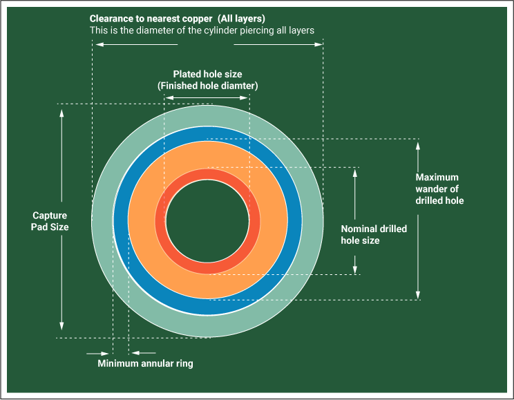
- Hole shadow: This is a cylindrical volume whose diameter is the drilled hole diameter plus the allowance for drill wander. This shadow is cast in all layers, and it is the surface used to compute insulation spacing to planes or traces.
- Plane layer: This is a copper layer that forms one of the layers in a PCB.
- Annular ring: This is the additional diameter of a capture pad over the minimum pad size that is required to exactly contain the shadow cast by the drilled hole. This additional copper is utilized to make a connection between a trace entering a pad and the hole plating. Also, this connection should never be the end-on cross-section of the trace, which can result in joint failure during soldering.
- Breakout: This is the condition where the drilled hole is so eccentric that it is not all contained within the capture pad. This can minimize PCB reliability by creating insulation thinner than required or by generating a butt connection (end-on) between a trace and a plated through-hole.
- Non-functional pads: These are pads on inner layers that are not required to connect a trace to a plated through-hole. Non-functional pads are not required in modern PCB fabrication operations.
Top-down view of the structure shown above:
The visible elements of the hole are shown in this diagram:
- Capture pads on the two outer layers
- Capture pads on the inner layers
- Drilled hole diameter
- Hole plating
- Shadow cast by the hole drilled through the board
- Plane clearance hole
What are the manufacturing and reliability considerations for pad design?
Ensuring a PCB pad stack design meets manufacturability and reliability requirements requires one to consider several factors:
- Maximum tolerances build up the minimum insulation between opposing conductors, which in this case refers to the hole plating and the copper in the trace and plane layers. They need to comply with the standards of the engineered product. For telecommunication equipment, a minimum insulation spacing of 4 mils is required, and for other products, it is 5 mils.
- There needs to be robust connections between traces and plated through-holes or vias.
- The aspect ratio needs to be such that the wall of the hole withstands the stress of the plating process without failure.
Even if you follow the guidelines above, drilled holes might not always pass through the board as specified. This might happen due to the following factors:
- Drill wander can occur where the drill can deviate from the preferred drilling axis (eccentricity)
- Alignment errors in the film layers
- Laminate shrinkage during lamination. This might lead to an error in locating the drill hole.
- Inaccurate registration of the layers during lamination
Drill wander is when drilled holes are off from where they are actually supposed to be. Each manufacturer would have reached a tolerance after going through its process, called drill tolerance. This drill tolerance is used to define the hole shadow of every drill hole.
High precision manufacturers can keep the tolerance down to ±5 mils, also known as TIR (total included radius). In the US, middle-tier manufacturers can keep this tolerance down to ±6 mils, and other manufacturers can hold it down to ±7 mils.
It is important for the PCB designer to know where the board will be manufactured to provide accurate allowances for the drill wander error. When it comes to high-volume production, drill wander tolerance should be much higher.
What are the differences between density levels A, B, and C in IPC standards?
Levels A, B, and C describe the measure of the relative ease of manufacturing in IPC standards.
The table below summarizes the differences:
| IPC Density Level | Component density | Footprint geometry | Typical applications |
|---|---|---|---|
| Level A | Low | Maximum | Used when board space is not constrained |
| Level B | Medium | Median | Suitable for reflow, wave, drag, and dip soldering; reliable solder attachment |
| Level C | High | Minimum | Ideal for high-density designs such as handheld and portable electronics |
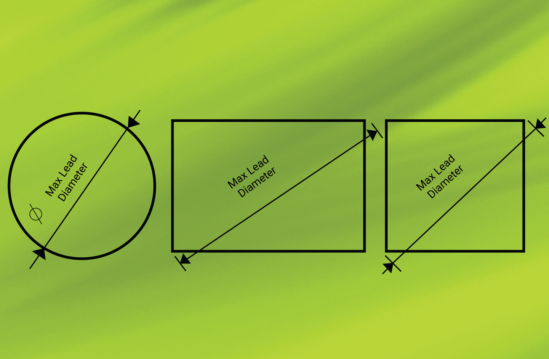
How to calculate PTH and pad diameters
The steps to compute through-hole and pad diameters are as follows:
1. Find the maximum lead diameter
You need to find the maximum lead diameter that is available in the package drawing or datasheet of the component. The maximum lead diameters for different shape types are as shown in the image below:
- The round PTH lead requires a round hole shape
- The rectangle PTH lead requires a rectangular hole shape.
- Square PTH lead requires a square hole shape.
2. Calculate the minimum hole size
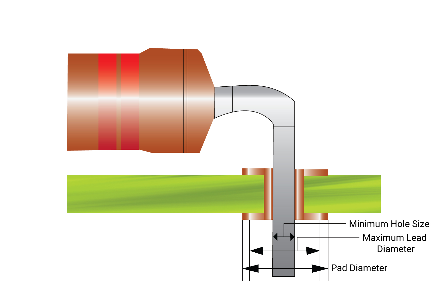
Minimum hole size is calculated according to the equations below:
For Level A of IPC-2222
Minimum hole size = Maximum lead diameter + 0.25mm (10mil)
For Level B of IPC-2222
Minimum hole size = Maximum lead diameter + 0.20mm (8mil)
For Level C of IPC-2222
Minimum hole size = Maximum lead diameter + 0.15mm (6mil)
3. Calculate the pad diameter
Post calculating the minimum hole size, you need to know that the minimum annular ring is 0.05mm (50um). According to IPC-2221, the minimum fabrication allowance is 0.6mm, 0.5mm, and 0.4 mm for Level A, Level B, and Level C, respectively.
Pad Diameter = Minimum hole size + Minimum annular ring x 2 + Minimum fabrication allowance.
For Level A of IPC-2221
Pad diameter = Minimum hole size + 0.1mm + 0.60mm (24mil)
For Level B of IPC-2221
Pad diameter = Minimum hole size + 0.1mm + 0.50mm (20mil)
For Level C of IPC-2221
Pad diameter = Minimum hole size + 0.1mm + 0.40mm (16mil)

Design for Manufacturing Handbook
11 Chapters - 96 Pages - 90 Minute ReadWhat's Inside:
- Annular rings: avoid drill breakouts
- Vias: optimize your design
- Trace width and space: follow the best practices
- Solder mask and silkscreen: get the must-knows
Download Now
What is the IPC-7251 and IPC-7351 padstack naming convention?
The padstack is represented by a combination of letters and numbers that stand for shape or land dimensions on different layers of boards. Such combinations are used in conjunction with the land pattern conventions according to the IPC-2220 design standards.
The first section of the padstack notation includes the land shape, written in lower case. There are 6 fundamental land shape identifiers.
b – Oblong
c – circular
d – D Shape (being square-shaped at one end and circular at the other)
r – rectangular
s – square
u – contour (refers to an irregular shape)
Padstack defaults:
- Solder mask is of a proportionate 1:1 scale of the land size
- The paste mask is of a proportionate 1:1 scale of the land size
- The assembly layer land is proportionately 1:1 scale of the land size
- The inner layer and outer layer land are of the same shape
- The primary and secondary lands are of the same size
- The inner layer land shapes, vias, and mounting holes are circular
- Thermal inner diameter, outer diameter, and spoke width sizes follow the IPC Level A, B, or C, with the thermals having 4 spokes
- Plane clearance and anti-pad size follow the IPC Level A, B, or C
Example:
- “c140h80”
- c denotes a circular land with a 1.40mm diameter
- h denotes a hole size of 0.80mm
- s450
- ‘s” denotes a square SMT land size of 4.50mm
Resources to calculate pad sizes
There are various specifications for pad sizes, such as the IPC-7351 standard, which details the required specifications. Other resources that you can use to calculate pad sizes include:
1. Pad and land pattern generators: Electronic design automation (EDA) tools today include pad and land pattern generators, also known as library wizards. Such software features are typically coupled with IPC standards and will automatically generate the shape and size of the pad required for components.
2. PCB design CAD vendor libraries: EDA tools also provide pre-made pad libraries and land patterns that can be downloaded and used. These are available to the users who have purchased a usage license of the design tool.
3. Third-party CAD library vendors: Users can purchase and download pads and land patterns from third-party PCB library component vendors. You may even find the pad and land patterns required, which have been created particularly for a component.
4. Pad and land pattern calculators: Designers and other users can easily find various pad and land pattern calculators online.
Design tip: Using industry-standard parts that are available online or generated automatically online can save a lot of time that might otherwise go into library creation. This also provides one with the added assurance that your CAD components are created according to industry or vendor specifications, meeting the fabricator’s DFM requirements.
Pads are a significant part of PCB design and manufacturing. The board designers need to master this to design fully functional and efficient circuit boards.
If you need to know more about pad design or have something to add, let us know in the comments!


