


Contents

On-demand webinar
How Good is My Shield? An Introduction to Transfer Impedance and Shielding Effectiveness
by Karen Burnham
In the era of miniaturization and HDI PCBs, space optimization on the PCB might frequently affect proper component placement. Appropriate component placement on a PCB improves the signal quality and performance of the device.
From a PCB assembly point of view, proper placement of components reduces the cost of production and reduces project production lead times while maximizing the operational efficiency of the PCB assembly. This makes PCB design considerations for component placement a critical part of the design process.
Check out our PCB component sourcing and stocking services to get your electronics to market fast!
This article outlines the aspects of proper component placement from a performance and production aspect. Also, how such aspects can decrease the turnaround time for a high-quality PCB assembly. Here are some aspects of strategies for proper component placement:
PCB floor planning
The first step in PCB layout design is to have a floorplan. A floorplan is a rough sketch that allocates general areas where blocks of circuitry and connectors are to be placed on the board.
What is a PCB schematic?
A PCB schematic is a fundamental two-dimensional circuit representation showing the functionality and connectivity between different active and passive components.
How can I improve my PCB design? With PCB floorplans!
The floorplan links the schematic drawing and the layout. It provides a head start to the designer on component placement. A pre-placement floorplan will allow the designer to optimize the component placement for signal integrity goals. Also, the small components, like bypass capacitors and termination resistors will be placed at an early stage instead of getting squeezed into the design at the end. The functional blocks of circuitry like power conditioning, RF, digital, analog, etc., should be arranged as groups to reduce signal crossing.
A floorplan gives an insight into how the signals flow between functional blocks. For an efficient board, group the power conditioning together so that their signals do not have to cross through sensitive areas of RF circuitry. Plan your placement to maintain the connection lengths as short as possible. The components that are part of high-speed signal paths where multiple nets connect a series of components should be placed as close together as possible. The designer has to consider the routing channels while planning the component placement to ensure there is adequate space. Check out our tutorial on how to place components in KiCad.
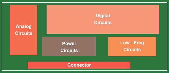
The requirements of power and ground planes should also be considered when planning out the placement of functional blocks of circuitry. Always implement continuous power planes unless there is a scenario where the design demands a split power plane. When dealing with split power planes, be cautious while placing the connected components across the split. The high-speed transmission lines should not cross the splits in power planes since it will break up the return path for those signals. Finally, avoid placing components of a different functional group in the midst of another circuit. For example, separate analog circuits from digital circuits. The figure below shows an example of a PCB floorplan:
If your layout has repetitive design blocks, auto-group the components to speed up the routing process. Read our article on 6 design mistakes that lead to PCB assembly errors to know more about the prevalent design pitfalls that can cause incorrect component placement.
Separating analog and digital circuits
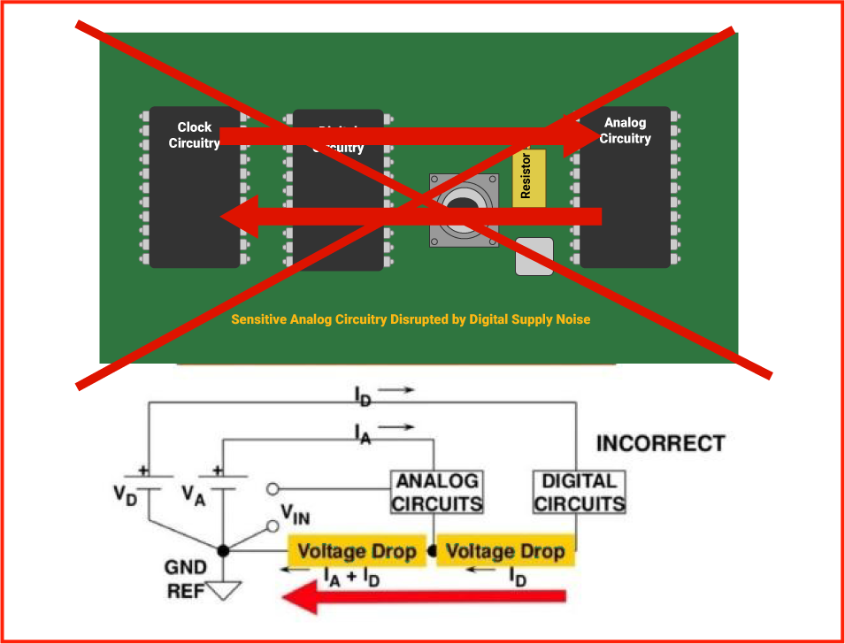
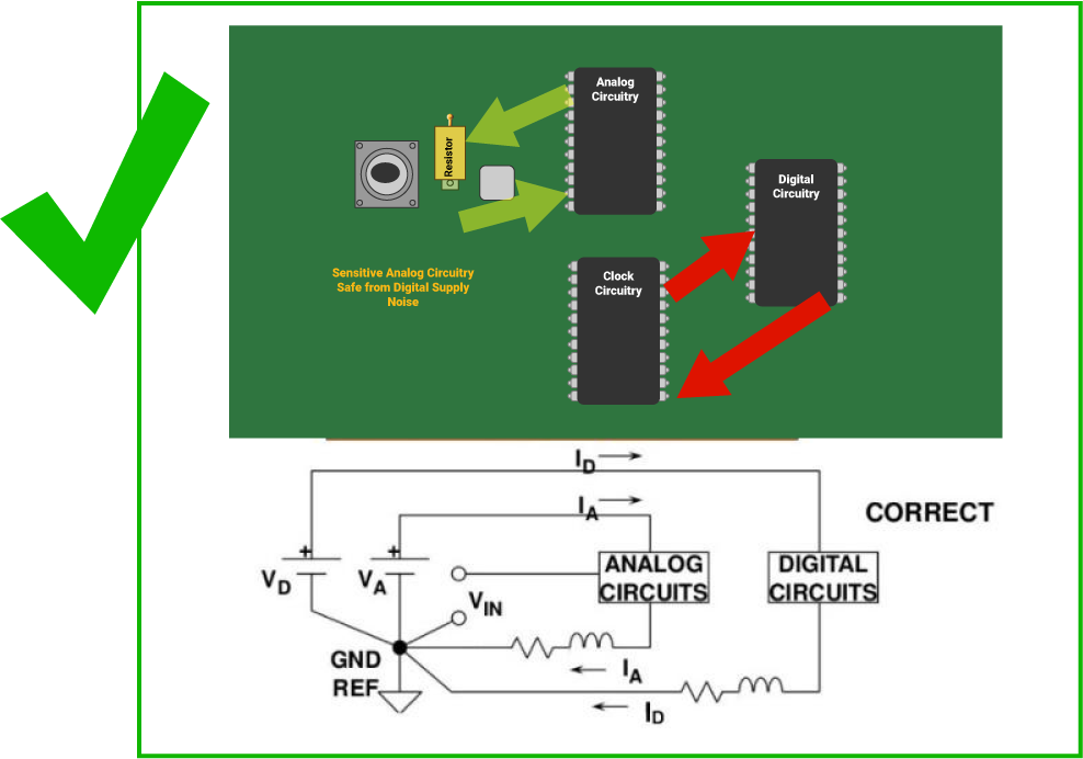
The placement routing topologies should be implemented in a way where the analog and digital GND do not mix up. The block diagram below shows the component placement. As we can observe in the first placement scheme, the analog and digital currents overlap each other. This degrades the analog signals due to crosstalk. The PCB designer must avoid such practices. In the second scheme, we can see the GND paths for analog and digital are isolated. Here, the digital return current does not interfere with the analog reference GND. The designer should adopt a placement strategy such that even if the GND is not isolated (same net), the currents of either section do not interfere with each other. To deal with crosstalks in HDI boards read how to avoid crosstalk in HDI substrates.
Component placement considerations in high-speed PCBs
As a first step, the designer should read the schematic and breakdown into sub-sections depending on the circuit function. For instance: analog, digital, high-speed, high-current, power supply, etc.
Apart from the circuit function, the voltage and current levels should be analyzed. Circuits with similar VCC and GND should be grouped and placed together.
Some of the component placement considerations are discussed below.
- To begin with, avoid placing sensitive high-speed devices close to the edge of the board. This is because the edge of the board possesses different impedance characteristics and also there is a higher chance of electromagnetic interference (EMI). On top of this, connectors that connect the PCB can radiate EMI. In view of these factors, it will be a good practice to place sensitive high-speed devices close to the board center to reduce the influence of EMI. For more on component placement standards, read our blog post on PCB Design for Assembly Checklist: 9 Important Checks for Layout Engineers.
- The thermal effect is another crucial aspect to be considered. In high-speed boards, the devices may run at a higher temperature than standard board components. To ensure that these hot components stay cool, implement a placement strategy in which these components receive unrestricted airflow. For instance, do not place bigger components like connectors in the path of airflow to a hot BGA.

High-Speed PCB Design Guide
8 Chapters - 115 Pages - 150 Minute ReadWhat's Inside:
- Explanations of signal integrity issues
- Understanding transmission lines and controlled impedance
- Selection process of high-speed PCB materials
- High-speed layout guidelines
Download Now
First place the critical components which have fixed locations like connectors
The component placement aspect of PCB design depends on the product housing, floor plan by the client, and the density & type of components used.
While starting placement a particular order should be followed:
- Assemble the connectors on the edges of the board as per design requirements and lock their position.
- Next, place the main functional chips like Microcontrollers, Opamps, Drivers, and Power supply chips, etc.
- Then place the auxiliary components such as crystals, decoupling capacitors close to the associated main chips.
- Place all the passive components like series resistors, Pull ups, ESD diodes, etc.
Some of the important factors that should be considered while carrying out component placement are listed below:
- Voltage & Current Levels
- Function types (Analog, Digital, Power supply, High speed,)
- Placement to facilitate the flow of High currents to minimize loops
- Power & GND distribution
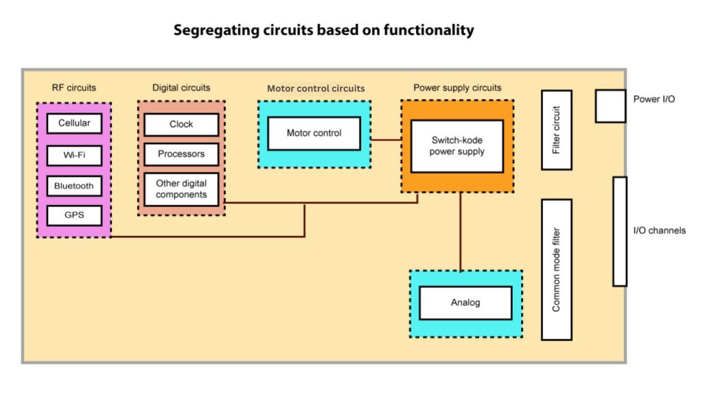
Apart from the circuit function, voltage & current levels should be considered. Circuits with similar VCC and GND should be grouped and placed together as shown in figure no (4). The different functioning sections are prioritized and placed. The most critical are in order of priority
- Wireless Wi-Fi, GPS
- Digital
- Motor control
- Power supply
Place the main components as per signal flow.
- Refer to the schematic circuit diagram while placing the components. Identify the main components of the circuit such as microprocessors, ethernet chips, memories, etc.
- Place these as per the floorplan and with the shortest traces between these main chips as per the datasheet guidelines and which makes the signal flow smooth and unidirectional as far as possible.
Place the associated components near the main components
- Next, place the components associated with the main components such as crystal oscillators, decoupling capacitors, termination resistors.
Placing components in close proximity could cause difficulty in the soldering and assembly process, thereby increasing assembly costs. For strategies to keep the assembly expense down, see how to reduce PCB assembly cost.
Termination resistors placement
In high-speed PCBs, the termination resistors must be placed along with the rest of the components instead of squeezing them in the end. Since termination resistors are part of the circuit as a whole, their placement is critical for the accurate operation of the circuit.
Here are two commonly used schemes for placing termination resistors:
Simple parallel termination
A termination resistor is placed on the end of the circuit nearest to the receiver while the other side is attached to the power or ground plane. Higher trace lengths from the load pin to the resistor will mean that the circuit will be more susceptible to signal reflection. Hence, the designer should place the resistor as close as possible to the load pin of the receiver to minimize the stub length of the connecting trace.

Series termination
The series resistor is attached inline after the driver pin of the circuit within lumped distance. Since the resistor is an inline part, it doesn’t have the stub length to be considered like in a parallel termination resistor. After figuring out the right strategy for placing the termination resistors, the designer can include it in the floorplan.
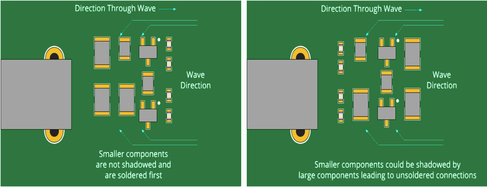
SMT and through-hole component placement
It’s advisable to place all the surface mount devices (SMD) on the same side of the board. All through-hole components should be placed on the top side of the PCB to reduce the assembly steps.
Further, high-speed memory modules (e.g., DDR5), AI processors, and advanced LiDAR sensors demand precise placement as any misalignment can cause signal interference, reducing processing efficiency. To achieve this, robotic-assisted surface-mount technology (SMT) is used to ensure micron-level accuracy in component placement for humanoid robotics PCB assembly.
Via shape considerations
In a high-speed circuit, any metal on the PCB should be considered as part of that circuit. The trace lengths, the via size, and the via depth should be taken into account for high-speed circuit calculation. The designer should understand that the via drill size impacts the size of the via. The smaller the vias, the better will be the performance of the circuit. Once the designer decides the vias sizes, the right placement of these vias close to their respective pads should be considered.
In high-speed design, the vias are placed closed to the pad to avoid parasitic capacitance. Sometimes they are placed partially on the pad or entirely within the pad. These adjustments require DRC adjustments.
To learn about pad design, read What is a Pad in PCB Design and Development?
Component selection and placement
It is good practice to minimize the use of sockets since they can introduce inductance. The designer should select the correct package, and accompanying component footprint while designing for high-speed. Components like op-amps are available in different packages. One type of op-amp may support shorter trace lengths in a circuit than the other. Finally, the component footprint shapes should be optimized for thermal considerations. The best way to dissipate heat is to place power pads right under the IC footprints that are connected to an internal plane. Even the smallest change in the pad shapes can tighten up the routing and decrease the connection lengths. This will result in a compact design.
To learn how to pick the right parts for your high voltage board, see how to select components and materials for power electronics PCBs.
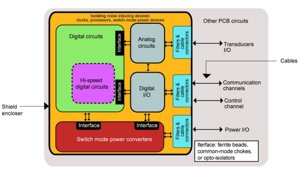
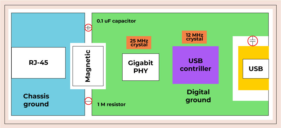
Ground plane isolation and surge suppressors placement
Isolate the ground planes when required in the digital section. The figure presented below shows the necessity of isolation within the digital sections. The USB and RJ45 connectors communicate externally. The board GND needs to be isolated to avoid any noise or interference from external chassis/body GND.
To protect circuits from external voltage surges often surge suppressing diodes and inductors are provided in the circuits. Place these surge suppressors close to the incoming signal connectors and avoid vias connecting these surge suppressors since these vias have parasitic inductances.
Read about via design in our article PCB Via Design Using Altium Designer
Component placement from an assembly point of view
Factors that affect component placement speed during assembly
The following factors directly affect the component placement speed during assembly.
Placement speed: the complete process of picking, inspecting, and placing the component on the board needs to follow standards to ensure optimal component placement speeds. By reducing the number of steps, one can increase the speed of placement. For example, if the components are oriented in a similar direction the components need not be rotated during placement, thus increasing the speed of assembly.
Part size: PCB components will vary in size. The manufacturer will have to consider the sizes of the components to decide the speed of the process accordingly. For every different part size, the pick and place tool will have to change.
Feeder capacity: The number of tape feeders that can be loaded into the machine at a time will directly affect the speed of the process. The size of the feeders will vary depending on the size of the component.
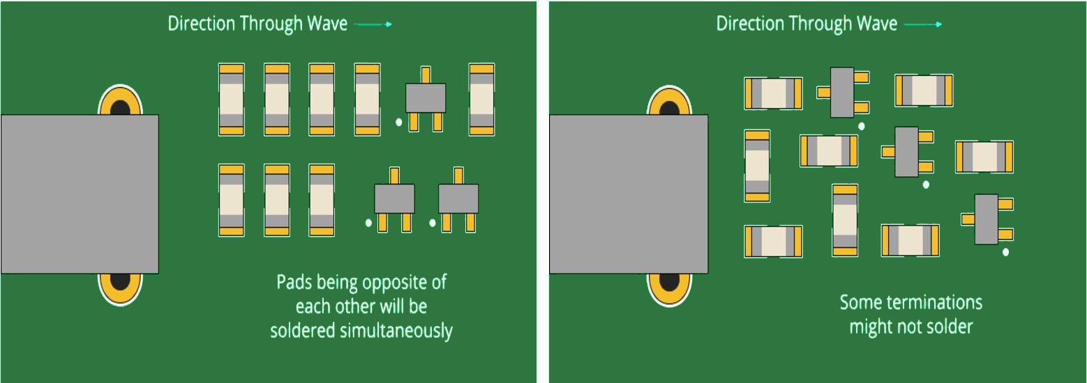
Component orientation
Align similar components in the same direction. This helps in effective routing in PCB design and ensures an error-free soldering process during assembly.

It is essential for manufacturers to oversee proper component placement in order to reduce downtime and turnaround time while streamlining the PCB assembly process. Component placement affects the performance of the device in terms of signal integrity and EMI and is taken care of during the PCB design. Similarly, the mechanical orientation of the component selection affects the assembly time and cost and therefore needs to be considered carefully. Executing the correct testing method proves to be beneficial in determining any wrong placement or faulty components.
To understand the fundamental things such as component selection, schematic checks, etc., required to produce a robust design read, mastering the art of PCB design basics.
Need help designing a cost-efficient circuit board? Post your questions and get them answered on our PCB forum, SierraConnect.


Start the discussion at sierraconnect.protoexpress.com