


Contents
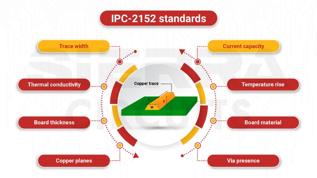
IPC-2152 is the standard for determining the current capacity, temperature rise, and width of a trace in a printed circuit board. It is an improvement over the existing IPC-2221 for optimizing the conductor size.
Released in 2009, it considers the impact of thermal conductivity, board thickness, dielectric material, and the presence of copper planes and vias on the conductor width. In this article, you will learn how to design your traces as per the IPC standards.
The current capacity of a trace determines its width
The maximum current capacity of a conductor is the amount of current it can carry without creating a hotspot or damaging the circuit. The line’s current capacity mainly depends on its width and thickness. Typically, every circuit construction begins by selecting a suitable default conductor size. It depends on the following factors:
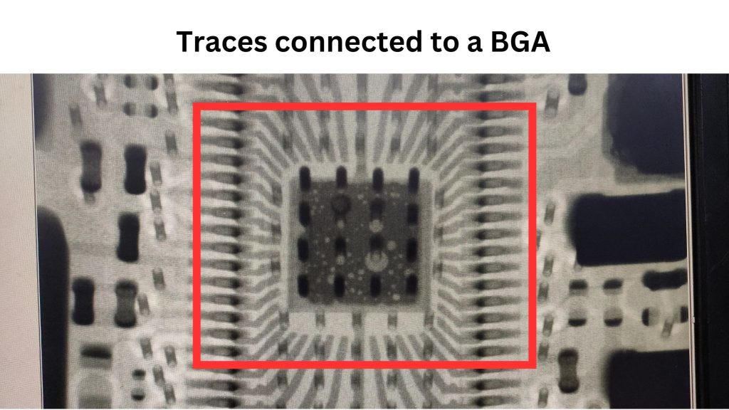
Trace cross-sectional area: This determines the power consumption of the signal line. During the manufacturing process, the fab house analyzes the cross-section of the conductor/trace using optical microscopy, X-ray imaging, focused ion beam, and 3D scanning. The image below shows an X-ray image of traces connected to a BGA.
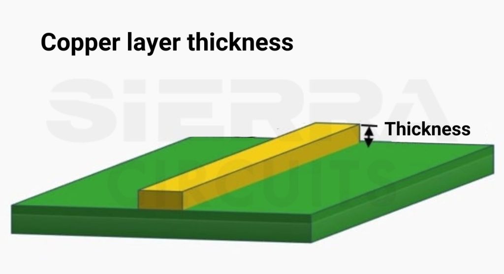
Copper layer thickness: It is the thickness of the copper layer used for creating the traces. This will significantly affect the electrical properties and cost of the board. Generally, the thickness ranges from 1 to 10 ounces per square foot.
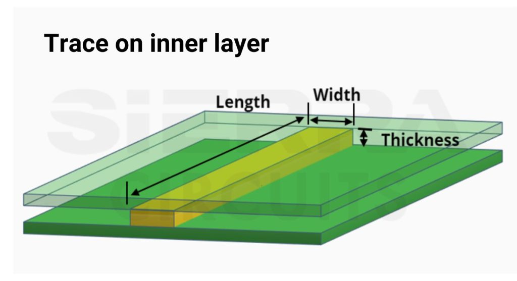
Trace location: The characteristics of the trace vary depending on its positioning in the inner or exterior layers.
What heats up a PCB trace?
Temperature rise in a circuit board creates hotspots, which can result in board failure. To limit the thermal issues, you will have to consider several factors, such as component density, power consumption of the circuit, dielectric material, supply voltage, and operating temperature.
One of the other significant parameters that impact heat generation is trace width. If the conductor is sufficiently wide (with low resistance and power consumption), there will be a lesser heat build-up. This means it should provide a low-impedance path for the current passing through it.
P = I² R gives the electrical power dissipated in the trace. This electric power gives rise to heat. If the surrounding environment does not dissipate this heat, the board can malfunction or even burn out. Even though the conductor temperature rises above ambient temperature, it should be sufficiently low. Furthermore, the ease with which the heat is dissipated from the board to the ambient temperature determines the thermal stability of the board.
Heat dissipation in a circuit board
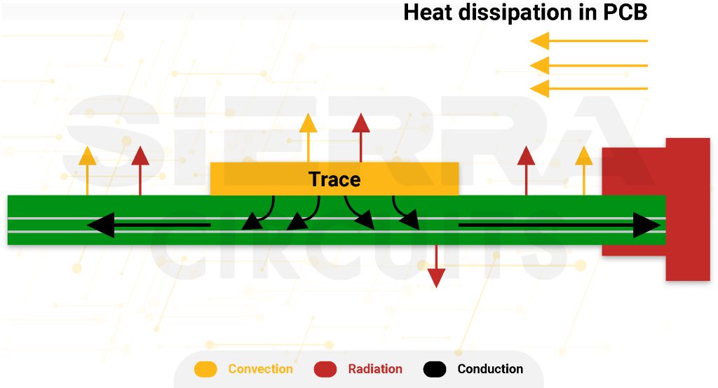
- Conduction: Heat transfer across a single or multiple types of materials in contact. It is mainly dependent on thermal conductivity, temperature difference, area, thickness, and geometry of the medium.
- Convection: Here, heat is transferred through a fluid medium. This can happen in two ways: natural and forced convection. In natural convection, heat dissipation happens when the surrounding air comes in contact, whereas forced convection involves implementing fans and pumps to circulate air.
- Radiation: It is the heat energy emitted from a higher-temperature material to a lower one through electromagnetic waves.
Normally, a 10°C temperature rise above the ambient temperature (25 °C) is allowed in a conductor. Although today’s PCBs have evolved drastically, the IPC 2152 standard is still implemented for thermal management, power budgeting, and energy efficiency analysis. Engineers also depend on the thermal testing of prototypes with thermal cameras, simulations, direct probing, and other techniques to ensure greater reliability.
What is the IPC-2152 standard?
Calculating the temperature rise of a PCB trace is a complex process. After a lot of testing and computer simulations, the IPC team created a 97-page document named IPC-2152. The guidelines are divided into two parts.
The main document deals with standards for conductor sizing, with charts and test results of external and internal conductors in varying environments such as vacuum and air. Next is an appendix that includes specific data on the impact of variables on the temperature rise in traces.
This standard provides information on the thermal characteristics of various conductor sizes. Some methodologies help in calculating the current carrying capacity of PCB conductors based on trace width, conductor thickness, and temperature rise. You can use this to ensure that the circuit designs can handle the electrical loads in real-world use and to prevent failures or damage due to excessive heat or current.

IPC Class 3 Design Guide
8 Chapters - 23 Pages - 35 Minute ReadWhat's Inside:
- IPC guidelines for manufacturing defects
- IPC standards for assembly processes
- Common differences between the classes
- IPC documents to set the level of acceptance criteria
Download Now
How to calculate PCB trace width based on IPC-2152
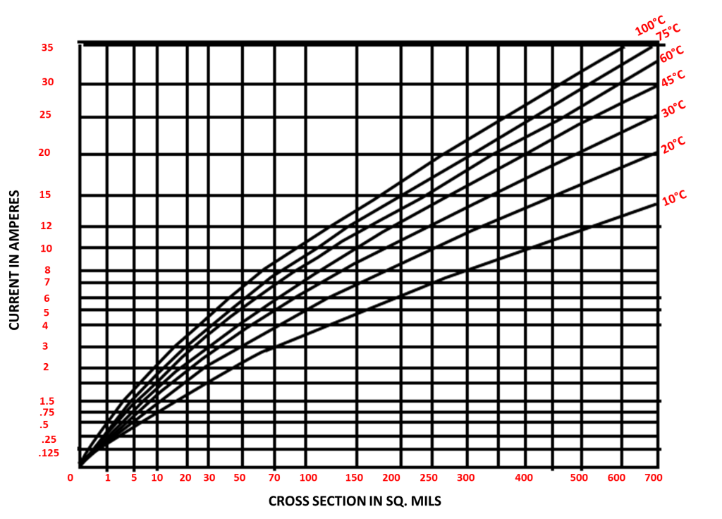
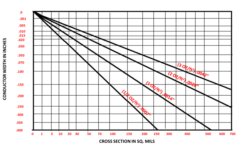
Using the charts provided in the IPC-2152 (section 5), you can calculate an unadjusted cross-sectional area of the trace based on the current capacity.
The next step is to determine the temperature rise. Normally, this is considered with respect to the ambient temperature, which is the temperature at which the board operates. But this is misleading, as there are many heat sources near the trace that affect the temperature rise in a circuit other than the ambient temperature.
Hence, IPC-2152 uses the term “local board temperature.” You need to decide on an appropriate temperature rise based on your design.
Finally, to get a more accurate value of the trace cross-sectional area, you need to multiply the chart value by the percentage change of each parameter, such as:
- Copper thickness multiplier
- PCB material multiplier
- Board thickness multiplier
- Plane multiplier
- Environmental modifier
Relevant charts for the above parameters are provided in the document. After you modify the chart value as per your design, calculate the trace width using the final cross-sectional area value. Instead of doing these complex manual calculations, you can use trace-width calculators that can provide instant results.
To learn more about PCB trace design, read our blog 10 best layout tips for high-speed and high-current PCB traces.
IPC-2152 calculator for circuit board design
While designing a circuit board, you need to consider many design aspects such as stack-up, signal integrity, thermal management, and conductor dimensions. To expedite this process, EDA tools include many calculators and simulators. However, only a few of these calculators cater to managing the thermal characteristics of a circuit. Currently, thermal calculators for computing the trace width are based on IPC-2152 and IPC-2221.

This free trace width calculator is based on IPC-2152.
Features:
- Three-in-one calculator. Computes trace width, maximum temperature rise above ambient, and current capacity
- Calculates resistance and voltage drop across a given trace length
- Supports multiple units for temperature and length
- Considers internal and external traces for computation
IPC-2221 vs. IPC-2152: which is better?
IPC 2152 and IPC 2221 set the primary guidelines for thermal management in a circuit. You need to be aware of these standards to build an efficient, and reliable PCB.
Features of IPC-2221 thermal standards
IPC-2221 covers a wide range of parameters of a circuit board design that include material, construction technique, electrical performance, and reliability.
It also provides thermal management guidelines for component placement, heat sink usage, and other cooling methods. This section provides information on the trace cross-sectional area, temperature rise, and current capacity.
In IPC-2221, the thermal parameters for traces were set by applying a known current and measuring the temperature rise of the trace on test boards. The results were summarized to create a formula that relates the copper area, temperature rise, and current capacity. Below are the graphs for calculating the trace width and cross-sectional area of the trace on internal and external layers.

I = k ΔT0.44 A0.725
Here,
I = maximum current capacity in amps
ΔT = temperature raised above ambient in °C
A = cross-sectional area in mils2
k = a constant depending on the position of the trace in the external (0.048) or internal layer (0.024)
When considering the formula, you can add a higher expected temperature rise that may result in overestimating the trace width required for the board. This also does not consider modern techniques such as large ground planes, copper pours, and heat sinks, which will remove the heat from heated components and high-current traces. This will result in the use of wider trace widths than required.
For more on high-current traces, read our blog how via stitching facilitates high-current PCB designs.
Features of IPC-2152 thermal standards
The IPC-2152 document solely interprets the industry standard for internal and external conductor size in relation to current capacity and temperature rise. It does not set any guidelines for other aspects of circuit board design, like IPC-2221.
IPC-2152 updates the conductor sizing charts and formulas that existed in IPC-2221, which was more than 50 years old. Additionally, the formula for the current capacity of the trace provided in the IPC-2221 standard was developed by considering a single-type board with a single copper weight. The IPC-2152 standard overcomes this by measuring the data from different board designs in different test situations. The improved parameters are:
- Copper weight
- Internal and external traces
- External environment (air or vacuum)
This new standard compiles the results into a graphical representation rather than summarizing them into a simple formula. From this benchmark, you can see the fact that the internal traces can carry higher currents, which are close to external traces.
Need help in designing reliable PCBs? Our engineering team can help you with thermal management, stack-up design, and DFM analysis.
You can book a meeting with our experts or call us at +1 (800) 763-7503.

Advantages of the IPC-2152 standard
- Improved electrical characteristics: This standard takes into account both the current capacity and temperature rise of the trace. Hence, the power consumption by the conductor will be under control, which will guarantee a reliable and desired electrical performance from the circuit.
- Consistency and replication: Calculation for a trace width provides consistent results that you can replicate in multiple designs.
- Limits the risk of defects: By optimizing the conductor width, you significantly reduce the risk of overheating, damage, and open circuits in the line.
- Time and cost savings: You can eliminate the risk of errors in manual calculations by using a systematic and automated approach of the trace width calculator. This will reduce board re-spins, which will save cost and time.
Download the DFM design guide to know more about optimizing the trace width and other design aspects.

Design for Manufacturing Handbook
11 Chapters - 96 Pages - 90 Minute ReadWhat's Inside:
- Annular rings: avoid drill breakouts
- Vias: optimize your design
- Trace width and space: follow the best practices
- Solder mask and silkscreen: get the must-knows
Download Now
Limitations of the IPC-2152 standard
- The calculations always assume the standard ambient temperature of 20°C. You have to adjust the results if the operating temperature is different. In the Sierra Circuits’ trace width calculator, you have the option to set different ambient temperatures to overcome this limitation.
- The standard does not consider the presence of multiple vias and their resistance, which can increase the overall resistance of the trace. Hence, you may require a wider trace for higher current capacity.
- IPC created this standard based on a test board made of polyimide material. Even though material properties are similar to FR4, there is a 2% difference.
Calculating via current using IPC-2152
In the article ‘Vias Are Cooler Than We Think’ of ‘Signal Integrity Journal’, it is seen that the via temperature rise will be less than the temperature rise in narrow traces. Here, the connected via can act as a small heat sink. On the contrary, the temperature rise in wider traces will be less than the via, hence the trace will act as a heat sink. This is due to the difference in thermal conductivity of the trace (air-exposed) and the via. The via will have enough plating as long as the minimum trace width adheres to the current capacity standard.
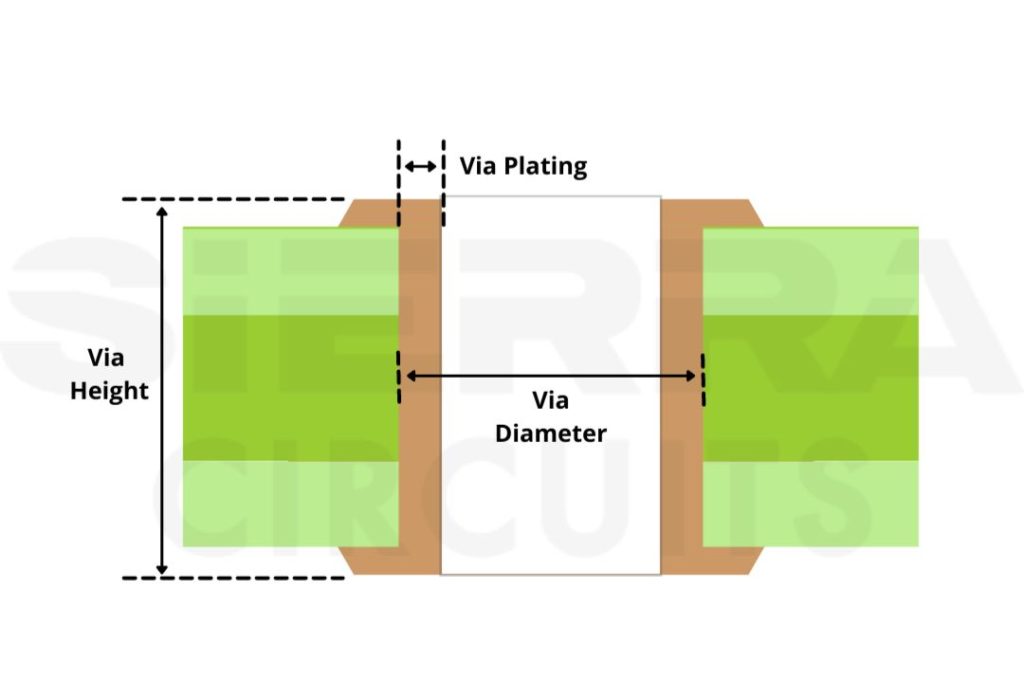
You can use Sierra Circuits’ via current capacity calculator to design an optimum via.
Features:
- Calculates three parameters: temperature rise above ambient, drill diameter, and maximum via current capacity
- Evaluates via resistance, voltage drop, and power loss
- Supports multiple units for input and output parameters
The IPC-2152 standard is an improvement over the IPC-2221 standard. It not only establishes the relationship between current, temperature rise, and trace width, but also considers many important design parameters such as via, material, board thickness, and thermal conductivity.
Even though the calculations become complex, you can use online calculators to optimize the trace width. If you have any questions on IPC-2152 or trace width calculation, please let us know in the comments. We will be happy to help you out.
About Sushmitha V : Sushmitha V has a master's degree in power electronics and has over four years of experience in the PCB industry. Her areas of interest include circuit board manufacturing, assembly, IPC standards, and DFM/DFA practices.


