What is a through-hole assembly?
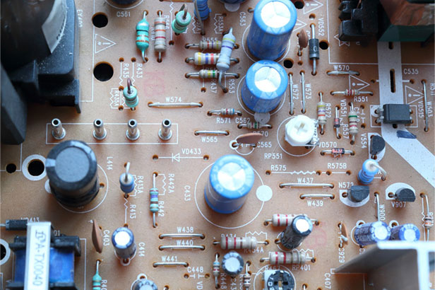
Through-hole assembly is the process of mounting leaded components to a PCB that involves drilled through holes. Later, the components are soldered to the pads on the opposite side of the board either by manual soldering or an automated soldering machine. The solder flux ratio is established carefully, as it is essential to maintain the quality of the solder joint between the pad and the component lead.
During the THA process, the component leads are inserted from the top of the board to the bottom through drilled holes, followed by soldering. These drilled holes could be plated through holes (PTH) or non-plated (NPTH). PCB manufacturers and designers should stick to IPC 610 A and J-STD-001 for through-hole assembly.
Why implement through-hole assembly?
Durable: A through-hole assembly process ensures a strong physical connection between the components and the board. This type of assembly provides a stronger bond and can resist environmental stress quite well. This is one of the reasons why they are incorporated in defense and space applications.
Preferable mounting technique for bulky components: THA is suitable for heavy components, such as electrolytic capacitors, semiconductor packages (TO-220), plug connectors, and relays that require additional mounting strength.
Support manual adjustments and quick replacement: It is easier to replace and adjust through-hole components than their surface mount counterparts.
Feasible for prototyping: Design engineers often prefer the larger through-hole in comparison to surface mount components when prototyping, since they can be easily used with breadboard sockets.
Good power handling: THA establishes a solid bond between the board and the components. This allows components to handle high voltage and high power with ease.

PCB Design for Assembly Handbook
6 Chapters - 50 Pages - 70 Minute ReadWhat's Inside:
- Recommended layout for components
- Common PCB assembly defects
- Factors that impact the cost of the PCB assembly, including:
- Component packages
- Board assembly volumes
Download Now
Through-hole assembly design considerations
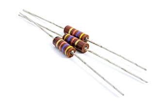
- Differentiate axial lead from radial lead components: Through-hole components are available in two types: axial lead and radial lead. In axial ones, the component terminal enters from one side and leaves from another side, passing through the center of the component, as shown below.
In radial, the component terminal enters and leaves from the same side, as shown below.
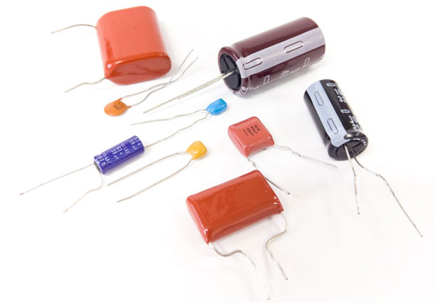
It is essential to understand the difference between the above component types because the axial lead components offer a flexible distance between two leads, while radial lead components indicate a fixed distance. And the radial lead components stand above the board, occupying less space than the axial.
- Quality of the solder joint: Always inspect the solder joint quality because it maintains the actual connection between the board and the component.
- Drill hole size: For drill hole sizes, the PCB manufacturer can make or bore the holes with respect to the aspect ratios of the board. It helps to maintain structural integrity.
Minimum hole size = Maximum lead diameter + 0.25 mm (for density level A)
Minimum hole size = Maximum lead diameter + 0.20 mm (for density level B)
Minimum hole size = Maximum lead diameter + 0.15 mm (for density level C)
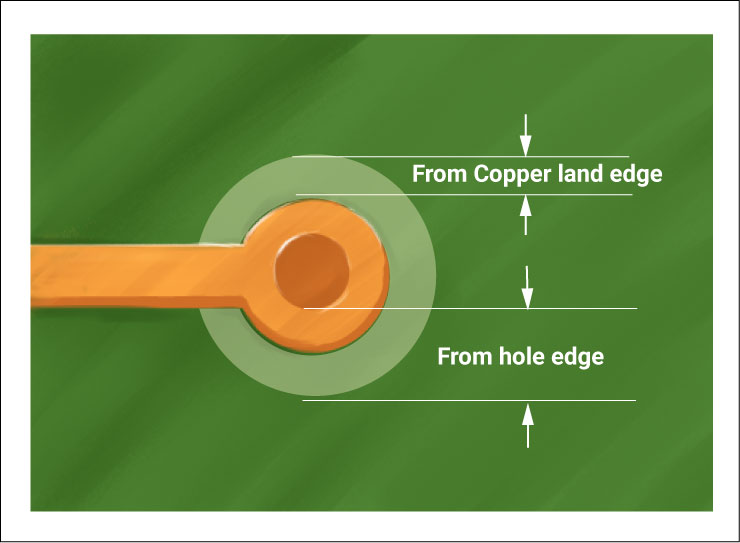
- Annular ring size: The diameter of annular rings should be adequate to provide a reliable solder joint.
- Pad size: According to IPC- 2221, the pad size for through-hole components is given by:
Pad diameter = [(Minimum hole size) + (2 x Minimum annular ring) + Standard fabrication allowance]
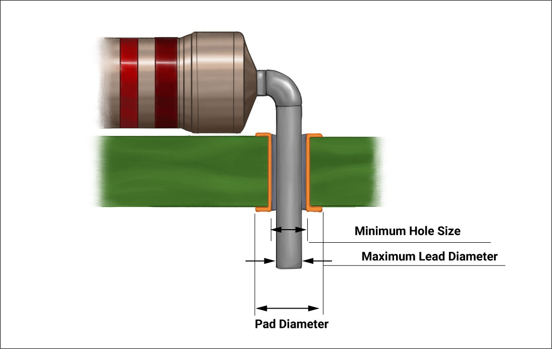
Note: Standard fabrication allowance is 0.6 mm, 0.5 mm, and 0.4 mm for levels A, B, and C density levels.
Pad diameter = Minimum hole size + 0.1 mm + 0.6 mm (for density level A)
Pad diameter = Minimum hole size + 0.1 mm + 0.5 mm (for density level B)
Pad diameter = Minimum hole size + 0.1 mm + 0.4 mm (for density level C)
- Solder mask relief: It is a tolerance parameter that specifies the optimum spacing between the solder mask and pads or annular rings. The standard value for solder mask relief is 4 mils. If not met, it will result in the uneven placement of the components.
- Solder fill: Although probably preferable, 100% solder fill is not necessary in all cases. For example, 75% fill is typically acceptable for class 2 and class 3 boards.
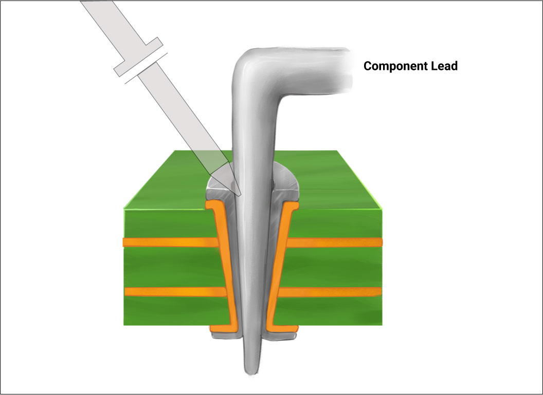
- Clearance: Adequate clearance inside the hole allows good solder flow through the board. Tight clearances could call for soldering from both sides, adding to the overall soldering time.
- Always provide separate drill files for both PTH and NPTHs if such holes are used.
- Mount flatter and smaller components first, then move to the larger and taller components.
- Use masking tape if the component leads are too short to bend.
- Make use of a conformal coating to avoid corrosion. And potting to ensure the mechanical and electrical stability of the components.
- For environment protection, check the RoHS capability of your manufacturer.
- The component terminal should be bent above the soldered area. This practice reduces both heat and solder requirements.
- There should be an even distribution of heat on the component lead and pad/hole so that the solder will adhere to both surfaces.
- During conventional PCB designing, parasitic capacitance and inductance affect the through-hole features. As far as 1 to 4-layer designs are concerned, through holes with diameters 0.36 mm, 0.61 mm, and 1.02 mm can be chosen respectively for via, pad, and the isolation area in the ground plane.
- For high-density boards, select through-holes with diameters of 0.20 mm, 0.46 mm, and 0.86 mm, respectively, for via, pad, and the isolation area in the ground plane.
- Place through-holes close to the power and ground pins for inductance improvement.
Also, see plated-through slots to properly accommodate rectangular leads and improve mechanical and electrical reliability.
Assembly fab notes
- Clearly place the reference designators near the component footprint. Typically, this is placed in the middle of the footprint in the assembly notes.
- Mention any height restrictions of the components on the board.
- Add special soldering instructions for connectors.
- Mention washable and non-washable components.
- While making the footprints, the body size, the lead sizes, and the orientation markings of the components need to be considered.
The through-hole assembly process can be time-consuming, but at the same time, it adds to the reliability and power handling of a board. The quality of the solder joint is also very important to have a long-lasting connection between the circuit board and the components.


