What is DFA in PCB design?
DFA or design for assembly is a structured process implemented to ensure the components are correctly assembled on a PCB without any malfunctions. Its secondary objective is to minimize the assembly costs of a board by simplifying its design.
Objectives of design for assembly
The goals of DFA are as follows:
- The components present in the BOM are available and are not obsolete or end-of-life products.
- The components’ manufacturing part numbers (MPN) match the footprint of the PCB.
- The component placement, sizes, and distances between the components are compatible with the assembly manufacturing processes.
- The solder mask and solder paste layers are valid and meet the production requirements.
- The DNI (do not install) components are correctly marked and verified.
What is the difference between DFM and DFA?
| DFA | DFM |
|---|---|
| Checks for the availability of components and ensures the assembly of components on the PCB is accurate. | Ensures that the PCB is manufacturable. |
| Checks the spacing between components and verifies whether the components can be soldered on the footprints on the board. | Checks for various manufacturing parameters such as trace width, spacing between the traces, drill size and so on. |

PCB Design for Assembly Handbook
6 Chapters - 50 Pages - 70 Minute ReadWhat's Inside:
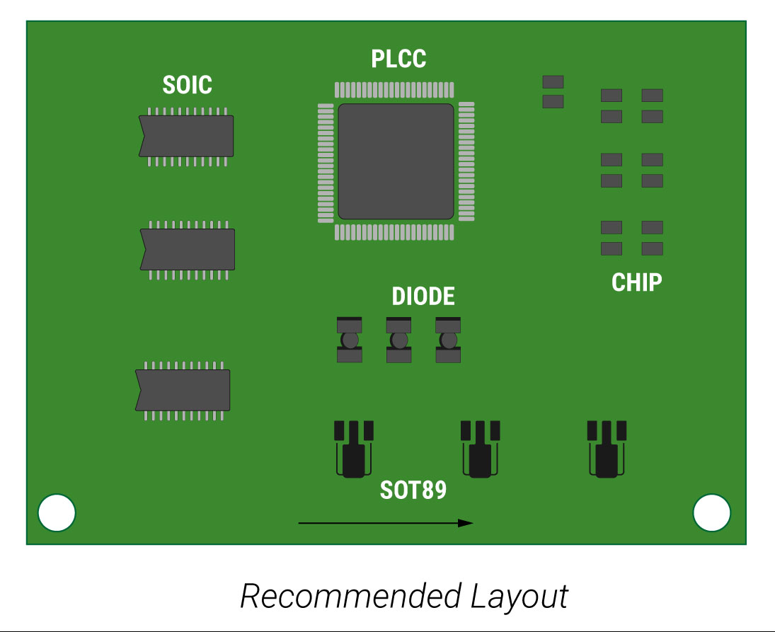
- Recommended layout for components
- Common PCB assembly defects
- Factors that impact the cost of the PCB assembly, including:
- Component packages
- Board assembly volumes
Download Now
DFA guidelines
Component footprint
The pads and the size of the footprint should be as per the component manufacturer’s datasheet. Here, the pin pitch, the hole sizes, the pad sizes, and the solder mask bridge sizes are considered.
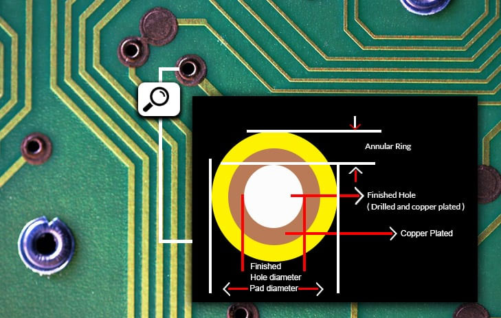
Pad size/Annular ring
Pad size should be a minimum of 0.010″ over the finished hole size for vias and 0.014″ over the finished hole size for component holes. Therefore, the annular ring (pad radius) needs to be a minimum of 0.005″ for vias and at least 0.007″ for component holes.
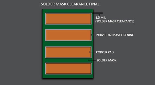
Solder mask clearances
Solder mask clearance is a permitted dimensional variation that decides how close the solder mask can be placed to the board surface features (copper traces). The purpose of this clearance is to offer sufficient spacing called solder dams between surface features that receive solder. This prevents the formation of solder bridges.
Component spacing
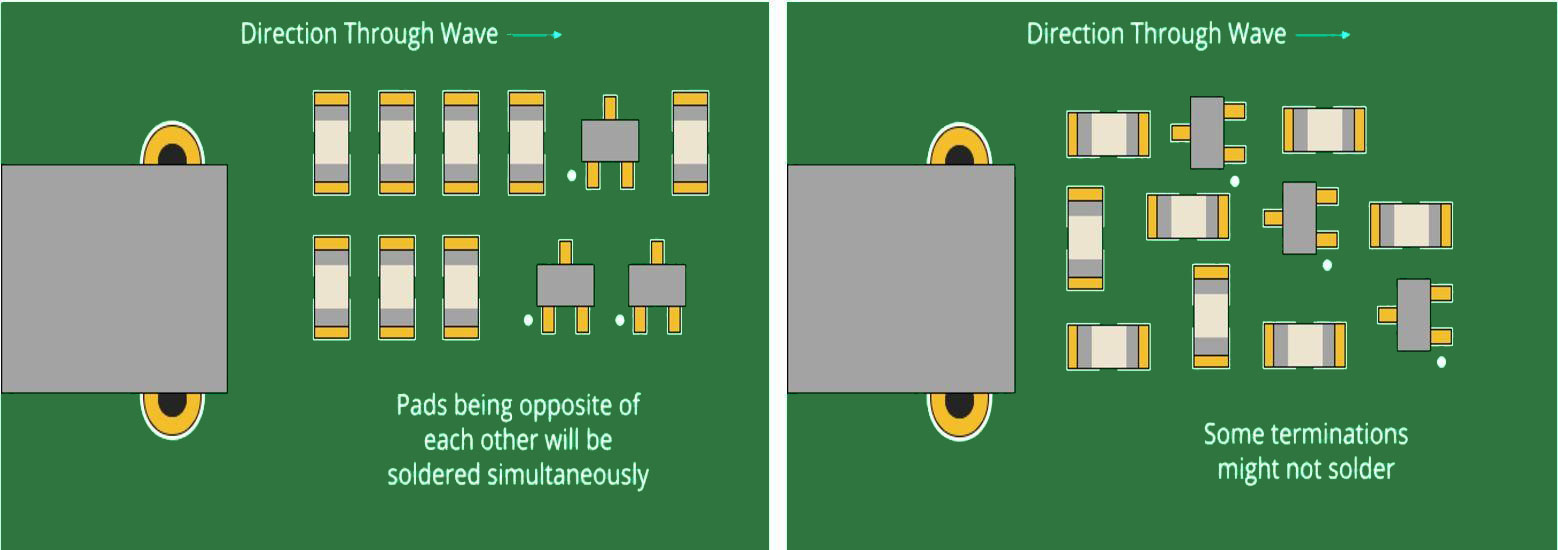
Part-to-part spacing
The land pattern spacing for all component packages will impact the cumulative timeline and reliability requirements for PCB assembly. For example, discrete components such as capacitors and resistors should always be spaced at least 10 mils apart, with 30 mils being the optimum distance. Adequate spacing between board components protects against faults like solder-bridging while allowing for easier rework processes. Do note that boards that require a smaller form factor will in turn have a smaller part-to-part spacing. The below table summarizes the optimum spacing ranges between various components.
| Chip | SOT | SOIC | PLCC | QFP | BGA | Axial | PTH | |
|---|---|---|---|---|---|---|---|---|
| Chip | 10-20 | 15-25 | 20-25 | 50-75 | 50-120 | 75-120 | 50-75 | 50-75 |
| SOT | 15-25 | 15-25 | 20-25 | 50-75 | 50-120 | 75-120 | 50-75 | 50-75 |
| SOIC | 20-25 | 20-25 | 30-50 | 50-100 | 75-120 | 75-120 | 50-75 | 100-150 |
| PLCC | 50-75 | 50-75 | 50-100 | 100-120 | 100-120 | 100-120 | 100-150 | 100-150 |
| QFP | 50-120 | 50-120 | 75-120 | 100-120 | 100-120 | 75-120 | 100-150 | 100-150 |
| BGA | 75-120 | 75-120 | 75-120 | 100-120 | 75-120 | 100-120 | 100-150 | 100-150 |
| Axial | 50-75 | 50-75 | 50-75 | 100-150 | 100-150 | 100-150 | 100-150 | 100-150 |
| PTH | 50-75 | 50-75 | 100-150 | 100-150 | 100-150 | 100-150 | 100-150 | 100-150 |
| **Dimensions given in this table are specified in mils | ||||||||
EMI and EMC considerations
Improperly designed PCBs might get affected by radiated electromagnetic energy called electromagnetic interference (EMI). To prevent this, board assemblies should be well organized and ensure components do not affect each other. This is will produce a good electromagnetic compatible (EMC) board.
You can prevent EMI issues by focusing on these design aspects:
1. Layer stack up
2. Trace routing
3. Analog and digital circuitry separation
4. Decoupling capacitors
5. Ground shielding
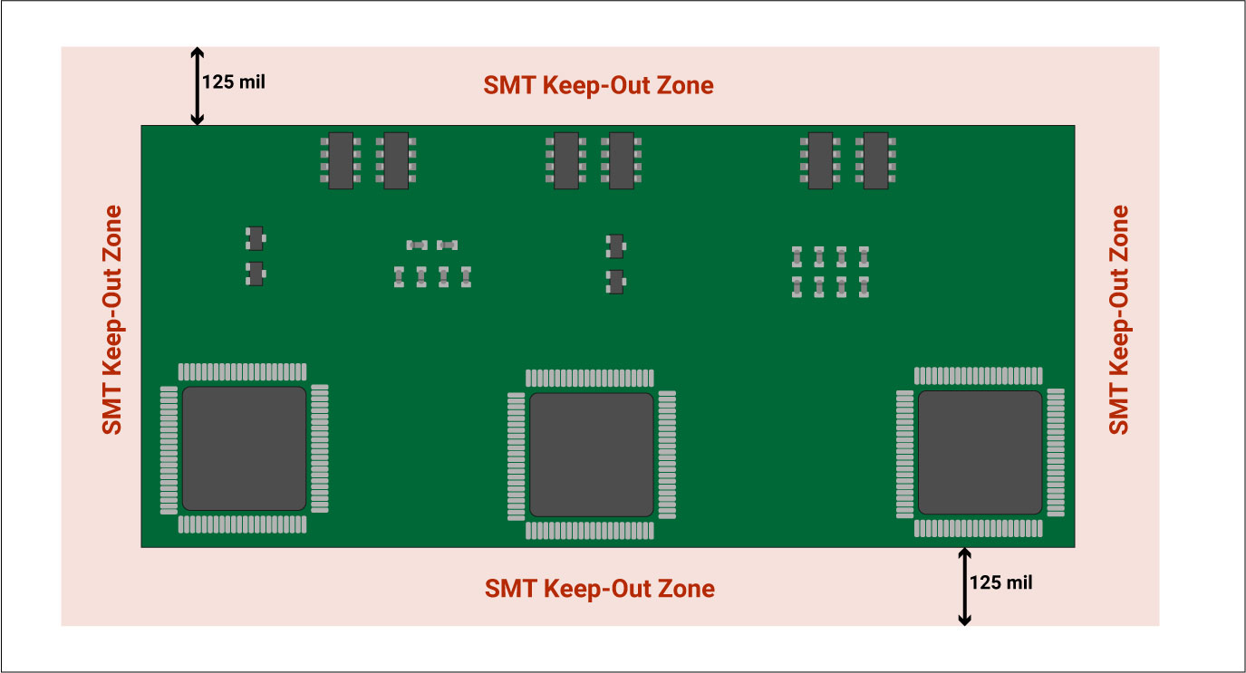
Part-to-edge spacing
The distance between the component on the board and the board edge is an important aspect to consider for the depanelization process. During the depanelization process, the parts close to the circuit board edge will experience stress which can damage solder joints.
It is a standard practice to widen the part-to-edge spacing on the board to accommodate the hold-down clamps in the solder application process. The clamps keep the board from moving while the solder paste is applied. When adequate spacing is not provided, the clamps could overlap the SMT components in this region leaving the board with insufficient solder paste. The inadaquate spacing could also damage the SMT parts.
Part-to-hole spacing
Part-to-hole spacing is needed for both through-hole parts and microvias. This requirement decides the minimum spacing between a component body/pad and either of the hole types. Part-to-hole spacing is categorized into two in quality assembly :
- Part-to-hole (component mounting hole) wall: This is calculated from the actual hole edge in the PCB to the pad edge. This is also known as drill to copper.
- Part-to-annular ring: This is estimated from the edge of the hole’s annular ring to the pad edge.
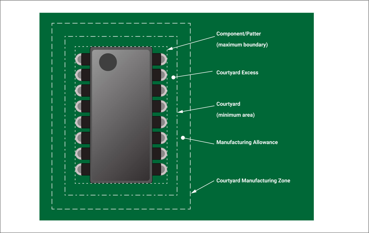
Component clearance
The maximum component boundary is the component’s outermost perimeter including the edge of the package and lead ends. The minimum pavement courtyard is specified around the part including the basic land pattern and the body.
The courtyard manufacturing zone is the outermost region that acts as a clearance for other parts, hardware, and the board edge. This region also offers space for rework.
- Unless otherwise defined, clearance is 0.25 mm.
- BGA devices require a clearance of 1.0 mm.
- Parts smaller than 0603 packages are required to have a 0.15 mm clearance.
- Connectors, crystals, and canned capacitors need a clearance of 0.5 mm, along with the clearance needed for mating connectors.
Component orientation
Align similar components in the same direction. This helps in effective routing and secures an error-free soldering process during assembly.
Manufacturers supervise component placement to minimize downtime and turnaround time while streamlining the PCB assembly process. Part placement impacts the device’s performance in terms of signal integrity and EMI. The mechanical orientation of the component selection affects the assembly time and cost and therefore needs to be considered carefully.
DFA best practices
- Opt for readily available components and ensure that they will be manufactured in the future. This will avoid future production delays.
- Adhere to component spacing guidelines. Component spacing defines which soldering technique is suitable for the board and what type of thermal dissipation is required.
- Use the footprints recommended by the component manufacturer. This should eliminate pad mismatches and provide proper markings and identification.
- Stick to the spacing clearances and tolerances that your manufacturer can handle. This assures that your design can be manufactured.
- Consider the circuit board’s operational environment. Through-hole components, which are more securely connected than SMDs, may be recommended for boards that are exposed to frequent movement or vibration.
- Make sure there’s adequate thermal relief used. This helps the board to withstand the soldering process.
Design for testing (DFT)
Design for testing, is an integral part of electronic production. Provisions must be made on the circuit board in the design phase itself. Usually, test points are provided so that the circuit may be probed.
PCB testing is done in two parts:
Pre-assembly (bare-board test)
- Isolation testing includes the calculation of the resistance between electrical connections.
- Continuity testing is where you check for open circuits, which is basically a variation on isolation testing.
- Short circuit testing includes checking for any undesired electrical connections due to manufacturing or design errors.
Post-assembly
There are two types of post-assembly testing:
In-circuit testing
In-circuit testing, electric probes evaluate the boards for opens, shorts, and values of capacitance, resistance, and other parameters. Instrumentation used for this includes a flying probe test (FPT) machine and bed of nails method of testing.
Functional testing
Functional board assembly testing is conducted at the end of the fabrication process to verify that the manufactured assembly does not fail immediately or has a shortened service life.
PCB functional test systems inspect the whole assembly, not just its components. This type of board testing simulates the operating environment of the assembly. Types of functional testing include:
- X-ray inspection
- Micro-sectioning analysis
- Solderability test
- PCB contamination test
- Time-domain reflectometer testing (TDR)
- Solder float test
- Peel test
DFA rules are part of standard practices to optimize assembly time and costs. Designer’s need to be aware of these rules so that the boards are efficiently assembled.


