Design for Manufacturing Handbook
The Designers' Handbook for DFM provides practical PCB design rules to help you build manufacturable circuit boards.


The Designers’ Handbook for DFM covers essential considerations, including drilling, aspect ratio, drill-to-copper clearance, vias, annular rings, solder mask, silkscreen, and tolerances.
In this handbook, you’ll learn:
- The fundamentals of design for manufacturability and its role in successful PCB production
- The differences between DFM, design rule checking (DRC), and design for testing (DFT)
- The design files and documentation required for a comprehensive DFM review
- Via design considerations, including aspect ratio, drill-to-copper clearance, and hole specifications
- Annular ring requirements for reliable plated through-hole (PTH) fabrication
- PCB fabrication tolerances and their impact on board quality and yield
- Guidelines for preparing production-ready output files and verifying manufacturing data
- Practical techniques for improving manufacturability throughout the PCB development cycle
The following sections walk through each topic in detail, showing how early design choices can simplify fabrication and reduce costly revisions.
What DFM checks are performed on your PCBs?
A DFM review evaluates your PCB design against manufacturing requirements to identify potential issues before fabrication. The review covers critical aspects such as drilling, vias, annular rings, conductor geometry, solder mask, silkscreen, and manufacturing tolerances.
Addressing these aspects before fabrication reduces rework, improves production consistency, and results in a more reliable PCB.
Drill checks
Drill checks verify that your hole sizes, drilling methods, tolerances, and clearances are compatible with the manufacturing process. These checks help identify potential plating, registration, and connectivity issues before the board enters fabrication.

The review considers both mechanical and laser drilling, along with finished hole sizes and drill tolerances. Since precise hole formation is essential to reliable vias and plated connections, these parameters directly influence PCB manufacturability and reliability.
It also verifies that different hole types (PTHs, non-plated through-holes (NPTHs), blind vias, and buried vias) are correctly defined and documented. Clear hole specifications and appropriate clearances ensure that each hole performs its intended electrical or mechanical function and minimize ambiguity during fabrication.
Aspect ratio
Aspect ratio determines the reliability of plated holes by influencing copper plating inside the hole. Vias that are small relative to the board thickness are more difficult to plate uniformly, increasing the risk of plating defects.
Maintaining an appropriate aspect ratio improves copper deposition inside drilled holes and reduces the likelihood of barrel cracks and other plating defects.
For through-holes, aspect ratio is the ratio of the PCB thickness to the drilled hole diameter. For microvias, it is the ratio of the drill depth to the drilled hole diameter. The ideal aspect ratio is 10:1 for through-holes and 0.75:1 for microvias.
Drill-to-copper clearance
Drill-to-copper clearance ensures there is adequate spacing between drilled holes and nearby copper features to prevent manufacturing defects. During a PCB DFM review, manufacturers verify that the specified clearance accommodates drill tolerances and minimizes the risk of damaging adjacent copper during drilling. Maintaining sufficient clearance improves fabrication reliability and helps prevent electrical and mechanical failures.
The fabricators also look for conditions that can compromise board quality, including inadequate drill-to-copper clearance, annular ring breakout, resin smear, burr formation, and excessive drill complexity. Addressing these issues before fabrication reduces rework, improves production consistency, and results in a more reliable printed board.
Annular ring
An annular ring is the copper area surrounding a drilled and finished hole that provides a reliable connection between the hole and the surrounding copper. Maintaining sufficient annular ring width accommodates drilling and registration variations and reduces the risk of breakout.
The required annular ring width depends on the finished hole size, drilling accuracy, and board construction. When the copper land becomes too narrow, drill wander can leave little or no copper around portions of the hole, increasing the risk of tangency, breakout, and unreliable plating. Following established annular ring design rules provides a larger process window while improving through-hole reliability.
During a DFM review, manufacturers verify that the designed annular ring meets applicable design rules and can be achieved with the manufacturing process. Identifying an insufficient annular ring before fabrication helps prevent connectivity and plating issues and provides a larger manufacturing process window.
Signal checks
Reliable electrical performance depends on conductor geometry that meets both design and fabrication requirements. In this stage, manufacturers evaluate trace widths, spacing, and routing to ensure the design can be manufactured consistently while meeting its electrical requirements.
Copper traces that are too narrow can increase resistance and become difficult to fabricate, while insufficient spacing between conductors can result in shorts or electrical breakdown. High-current traces require adequate width to carry the expected current without excessive heating, and high-speed signals may require controlled impedance and consistent routing to maintain signal integrity.
Reviewing conductor geometry before fabrication helps identify routing issues, improve electrical performance, manufacturing yield, and the long-term reliability of the board.
Solder mask
A PCB DFM review verifies that solder mask clearances, openings, and dam widths support reliable fabrication and assembly. Properly designed mask features protect exposed copper, prevent solder bridging, and improve solder joint quality.
Insufficient solder mask clearance can expose unintended copper, while narrow solder mask dams may not be manufacturable and can lead to solder bridging between adjacent pads. Properly defined solder mask openings improve insulation, reduce the risk of solder defects, and protect the underlying copper from environmental exposure.
Reviewing solder mask features before fabrication helps prevent assembly issues, improves solder joint quality, and increases the long-term reliability of the finished PCB.
Silkscreen
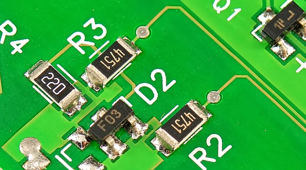
Clear and accurate silkscreen markings improve assembly, inspection, and troubleshooting. Manufacturers evaluate the placement of reference designators, polarity indicators, logos, and other printed markings to ensure they do not overlap pads, vias, or other features that could affect assembly.
Poorly placed silkscreen can become unreadable after assembly or interfere with soldering when printed over exposed copper or solder mask openings. Maintaining adequate clearance between silkscreen and conductive features improves legibility and helps prevent manufacturing and assembly issues.
Reviewing silkscreen features before fabrication ensures component markings remain visible, supports accurate assembly and inspection, and improves the overall quality of the finished PCB.
How to design vias for reliable PCB performance?
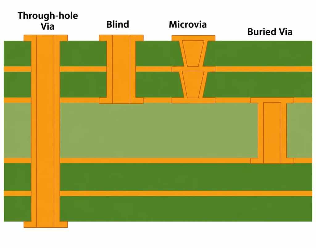
Select the appropriate via structure based on your board’s routing density, signal integrity requirements, and stack-up. Choosing the right via technology improves routing efficiency, supports high-speed signals, and helps meet the electrical and mechanical requirements of the finished printed circuit boards.
Standard through-hole vias are widely used to connect signals between the outer and inner layers, while blind and buried vias provide additional routing flexibility in high-density designs. For HDI applications, microvias enable finer routing and smaller component pitches, making them well suited for compact, space-constrained products.
Designs with high pin-count BGAs or high-speed interfaces often benefit from via-in-pad plated-over (VIPPO) technology. By placing the via directly beneath the component pad, designers can shorten signal paths, reduce parasitic effects, and improve routing efficiency. Back drilling removes excess copper from unused via signal paths to minimize signal reflections and maintain signal integrity in high-speed circuits.
Selecting the appropriate via structure early in the design process allows designers to balance electrical performance, board complexity, and fabrication capabilities while avoiding unnecessary manufacturing challenges.
Why do PCB manufacturing tolerances matter?
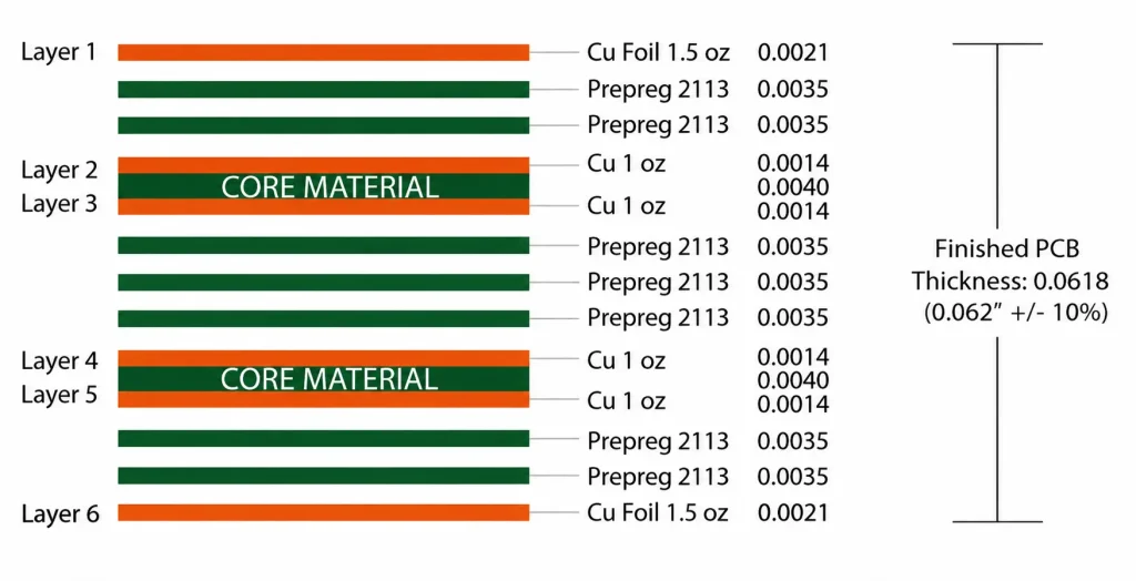
Circuit board manufacturing tolerances define the acceptable variation in critical dimensions while ensuring the finished product performs as intended. Understanding these limits allows designers to create layouts that align with fabrication capabilities and reduces the likelihood of dimensional variations affecting board performance.
Key tolerances apply to board thickness, copper thickness, conductor width, trace spacing, and drilled holes, all of which influence the accuracy of the fabricated PCB. Features such as annular rings, solder mask openings, and layer-to-layer registration must also remain within specified limits to maintain proper alignment and electrical connectivity throughout the board.
High-speed and high-reliability designs often require tighter process control. Controlled impedance traces depend on consistent material thickness and conductor geometry. Bow and twist tolerances help ensure the assembled PCB remains mechanically stable during component placement and soldering. Designing within these established limits improves fabrication consistency and supports reliable board performance across production.
How should you prepare your manufacturing data for production?
Generate complete, accurate, and up-to-date manufacturing files as the final step in your circuit board design workflow. A thorough data check helps uncover polarity errors, missing layers, outdated revisions, and other inconsistencies that could affect downstream manufacturing.
Inside this design guide, you’ll learn how to:
- Inspect Gerber, ODB++, and drill files for completeness.
- Check layer sequence, board outline, and polarity before submission.
- Review solder mask and silkscreen outputs for accuracy.
Download the full design guide to learn more.
How can you ensure your designs are manufacturable?
Integrate DFM practices into every stage of the development cycle instead of treating DFM as a final verification step. Evaluating fabrication capabilities early, following established design rules, and validating design data throughout the project reduces rework and supports a smoother transition to fabrication.
This handbook shows you how to:
- Consider fabrication capabilities during stack-up and layout planning.
- Apply PCB DFM checks throughout the design cycle instead of waiting until the end.
- Validate manufacturing data before releasing the design.
- Communicate design intent through complete documentation.
- Resolve potential fabrication issues before they affect production.
The Designer’s Handbook for DFM brings these best practices together in one resource, helping designers create layouts that are easy to fabricate, assemble, and verify while reducing costly revisions.
Download Sierra Circuits’ Designer’s Handbook for DFM to learn practical design guidelines, fabrication requirements, and review techniques that help you deliver production-ready PCB layouts with greater confidence.