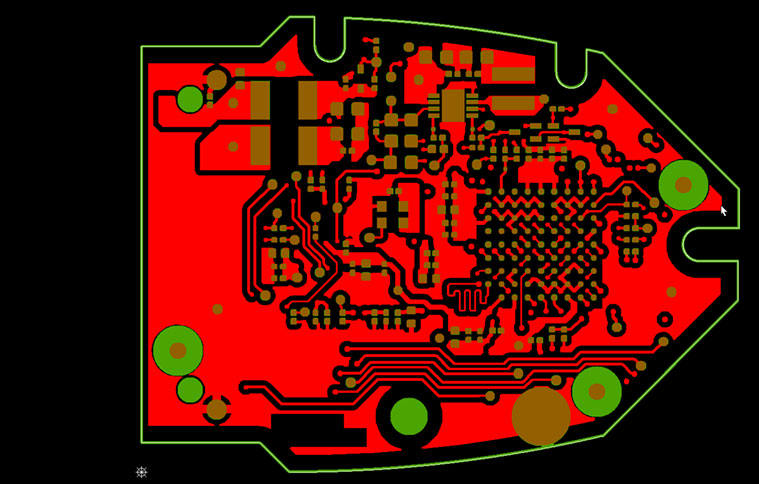
PCB manufacturers receive the designer’s data in various file formats before production begins. These files contain information about the board layer orientation, component insertion, wire wrapping, routing, IPC netlist, drill files, and many other design specifics. It is very important to analyze these production files to ensure an error-free manufacturing process. This analysis can be automated by using CAM software.
What is computer-aided manufacturing (CAM)?
Computer-aided manufacturing automates the manufacturing process using software and computer-controlled machinery. It examines the design files and recognizes the format. Later, the artwork layers and the drilling data are also analyzed. CAM is also responsible for design rule checking (DRC) that determines whether a design meets the manufacturing standards.
CAM configures the best component orientation to improve material utilization and machine efficiency.

Design for Manufacturing Handbook
11 Chapters - 96 Pages - 90 Minute ReadWhat's Inside:
- Annular rings: avoid drill breakouts
- Vias: optimize your design
- Trace width and space: follow the best practices
- Solder mask and silkscreen: get the must-knows
Download Now
Data output from PCB CAM
CAM system numerically control the drilling data and component placement parameters. A computer-based regulator interprets a sequential list of codes into instructions that will be understood by the machine tools.
The CAM system performs the following steps:
- Inputs digital data in the form of Gerber, Excellon, etc.
- Reconstructs a prototype of the PCB.
- Checks for manufacturing violations or errors and communicates with the designer if required.
- Sends product information to ERP (enterprise resource planning) for quoting.
- Sends product details to the engineering department, which will determine how and on which machinery the board will be manufactured, and produce the travelers.
- Adjusts the DFM (design for manufacturing) as necessary, and discuss changes with the designer.
- Prepares the customer and the production panel.
- Adjusts for deviations in the manufacturing process (for example, scaling to compensate for distortions during lamination).
- Sends manufacturing data to ERP.
- Outputs digital data modules like photo plotting, direct imaging, legend printing, drilling, routing, scoring, AOI, and electrical test files.
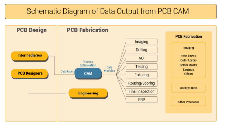
This entire concept summarizes computer-assisted manufacturing.
Significance of the coordinate system
Design files are the input for a manufacturer’s CAM system to restructure a model of the circuit board with the correct alignment of all the layers. CAM software will improve board paneling. It will mirror, rotate, scale, and shift as needed by the production.
Mirroring or flipping the layers should be strictly avoided. All layers should be viewed from the top of the circuit board (this means that the text has to be readable on the top and mirrored on the bottom layer).
All files in the manufacturing data such as copper, drill, route, solder mask, legend, etc. are read into the CAM software. All these layers should align correctly. This alignment can be achieved by releasing all the files in the same coordinate system. After being read into the CAM software, they automatically align.
In some cases, registration can be accomplished by adding alignment targets to images. But, this is not the solution. Such complications related to misalignment can be eliminated by using the same coordinate system.
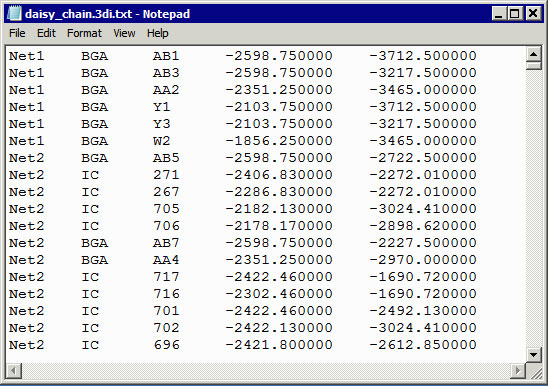
PCB netlist
A netlist is the basis of a PCB layout and the specifications are defined in IPC-356. It is a set of networks that define a bare board’s conductivity interconnection pattern. Generally, the netlist is an ASCII text file that comprises the CAM system instructions such as net names, pins, and XY coordinates of the start and endpoint for each net or node.
Netlist prevents software or operator error, thereby avoiding mistakes in data transfer. The customer’s CAD netlist will be compared by the manufacturer with the list obtained from the Gerber data. If there are any discrepancies in the data, we will assist the customer to fix them.
It is essential to include an “IPC-D-356 A” file in the data set. An example of a netlist text file is shown below.
What are the benefits of using CAM?
CAM offers the following benefits:
- User-friendly software
- Offers higher speed and efficiency that enables you to develop error-free prototypes
- Automates the production process and reduces the turn time
- Available in various electronic formats
All of the above-listed advantages help your manufacturer to speed up the circuit board fabrication process.


