Different types of vias can be drilled on a PCB stack-up. A via is implemented in a circuit board for providing electrical interconnection between its layers. The components and traces conduct signals through these vias, and hence they form the conducting channels through board layers. Blind and buried vias increase the connectivity and at the same time occupy very little space.
What are blind and buried vias?
Blind and buried vias are controlled depth vias commonly used in HDI boards. Here interconnection is established without consuming more space on the PCB, thus making more room for the increased wiring density. Since through-holes consume more board real-estate, the space available for wiring is reduced. Hence, blind and buried are preferred.

HDI PCB Design Guide
5 Chapters - 52 Pages - 60 Minute ReadWhat's Inside:
- Planning your stack-up and microvia structure
- Choosing the right materials
- Signal integrity and controlled impedance in HDI
- Manufacturing considerations for higher yields
Download Now
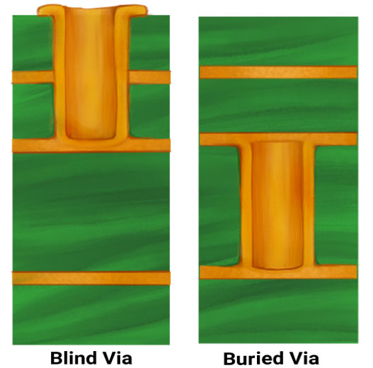
Blind vias
Blind vias start from an outer layer and terminate at an inner layer. These vias do not go through the entire board stack-up. They connect at least one inner layer of the circuit board with the outer layer. Top and internal layer or bottom and inner layer. Once these vias are laminated, the other end will not be visible, and that is why they are called blind vias.
Buried vias
Buried vias are also called hidden vias since they are not visible when observed from the external layers. These vias are meant for connecting the inner layers of the circuit board. Therefore, space will be available on other layers for wiring.
The IPC standards suggest that the diameter of the blind and buried vias should be 6 mils (150μm) or less.
How are blind and buried vias created?
For drilling blind and buried vias, controlled-depth drilling methods are chosen.
The drilling process of controlled depth blind vias is quite similar to that of the through-holes. The only difference is that the drilling source is programmed to stop after one or two layers. Care should be taken to ensure that the drilled hole does not have any connection with the layers underneath it. Then the hole is copper plated and made conductive.
Before drilling buried vias, the inner layers are drilled first. Next, the other layers are pressed to complete the stack-up.
Important guidelines when designing a blind/buried vias
While placing vias in your PCB design, follow these guidelines:
- These vias should always span an even number of copper layers.
- Blind vias should always begin at the top/bottom layer of the stack-up
These vias when compared to conventional through-holes are very effective in increasing the space available on a board for component placement.


