Following standard PCB component placement rules will expedite the assembly process. The easier the component placement, the faster will be the board assembly. While placing components in a circuit board design, a few aspects, like floor planning, component spacing, etc., should be kept in mind. These aspects are discussed below.
How to arrange components in a PCB?
The input and output board connectors strongly influence component placement on a PCB. Initially, the placement of these connectors is decided. Subsequently, the other components are placed depending on the flow of the signals. To aid placement, a rough PCB floor plan of the components is prepared. The circuit board floor plan and the schematics serve as the basic outlines for placing electronic components.
The floor plan demonstrates the way the signal moves between different functional blocks on the board.
The schematic is a circuit representation that shows how different active and passive components are connected to the circuit board. Hence, by referring to both of these, you can efficiently arrange components on a board.
8 important floorplan guidelines
- The board outline is first decided and imported into the PCB design tool.
- The input and output connectors that have fixed locations are then placed on the board, normally on the edge of the PCB.
- ESD and circuit protection components are then arranged close to the associated connectors.
- Group the power conditioning components to avoid their signals affecting the sensitive areas of the RF and analog circuitry. These are also placed close to the input power connectors.
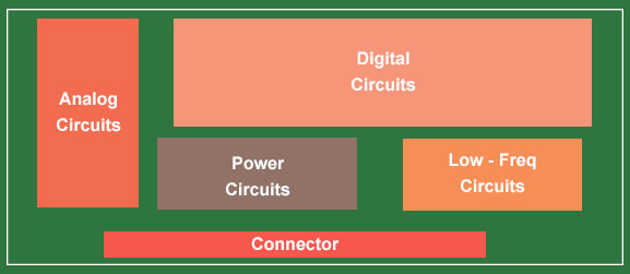
- Separate analog circuits from digital circuits.
- Place the main components such that the connection lengths between the components are as short as possible.
- Next, place the auxiliary components near the main components, such as decoupling capacitors, crystals, and series, as well as pull-up resistances.
- Continuous power planes should be used (split power planes are not recommended).
8 things to consider when placing components
As a PCB designer, you need to follow these guidelines to ensure that the placement does not negatively affect the operation of the PCB.
1. Through-hole component placement: Place all through-hole components on the top side of the board.
2. Surface-mount component placement: Keep all SMDs on the same side of the board, if possible.
3. Order of arrangement: All the connectors should be placed first, on the edge of the circuit board, along with ESD and circuit protection components. Next, the main functional chips, like microcontrollers, followed by auxiliary components, such as decoupling capacitors, should be placed. Finally, all the passive components, such as resistors, should be mounted.
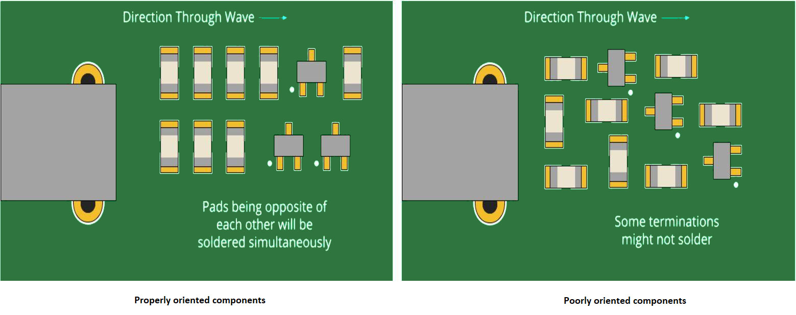
4. Component orientation: All similar components should be placed in the same orientation. This will help in easy routing, faster soldering, and rapid placement by pick-and-place machines.
5. Part-to-part spacing: If you place the components too close to each other on a circuit board, it will create many problems that will lead to redesign and refabrication. Hence, while placing the components, strictly follow the part-to-part spacing guidelines. The table below shows the recommended part-to-part spacings for different types of components.
| Chip | SOT | SOIC | PLCC | QFP | BGA | Axial | PTH | |
|---|---|---|---|---|---|---|---|---|
| Chip | 10-20 | 15-25 | 20-25 | 50-75 | 50-120 | 75-120 | 50-75 | 50-75 |
| SOT | 15-25 | 15-25 | 20-25 | 50-75 | 50-120 | 75-120 | 50-75 | 50-75 |
| SOIC | 20-25 | 20-25 | 30-50 | 50-100 | 75-120 | 75-120 | 50-75 | 100-150 |
| PLCC | 50-75 | 50-75 | 50-100 | 100-120 | 100-120 | 100-120 | 100-150 | 100-150 |
| QFP | 50-120 | 50-120 | 75-120 | 100-120 | 100-120 | 75-120 | 100-150 | 100-150 |
| BGA | 75-120 | 75-120 | 75-120 | 100-120 | 75-120 | 100-120 | 100-150 | 100-150 |
| Axial | 50-75 | 50-75 | 50-75 | 100-150 | 100-150 | 100-150 | 100-150 | 100-150 |
| PTH | 50-75 | 50-75 | 100-150 | 100-150 | 100-150 | 100-150 | 100-150 | 100-150 |
| **Dimensions given in this table are specified in mils | ||||||||
6. Separate lead-free and non-lead-free components: Lead-free components are not supposed to be mixed with non-lead-free counterparts.
7. Weight distribution across the board: The weight distribution across the board should be uniform. This can be achieved by placing large components in such a way that the weight is distributed throughout the board rather than being confined to a particular section.
8. Independent pads for every connection: Have independent pads for all the component connections. The size of each pad should be in proportion to the other pads.
Component placement tips for high-speed PCBs
Here are a few tips for placing parts in high-speed circuit boards:
- Place circuits with similar Vcc and GND together.
- Do not place sensitive high-speed components at the edge of the board. This reduces EMI.
- To avoid overheating of components in high-speed boards, place them such that they have enough space for free airflow. This will assist in heat dissipation.

High-Speed PCB Design Guide
8 Chapters - 115 Pages - 150 Minute ReadWhat's Inside:
- Explanations of signal integrity issues
- Understanding transmission lines and controlled impedance
- Selection process of high-speed PCB materials
- High-speed layout guidelines
Download Now
These are a few of the important guidelines for the placement of components on a circuit board. This will help in getting a better yield. To learn more, see component placement guidelines for PCB design and assembly.


