Copper is one of the most important elements in a PCB. Copper foils serve as conductive layers. If you look closer, you can see the copper tracks etched on circuit boards through which signals flow.
What is a copper-clad laminate?
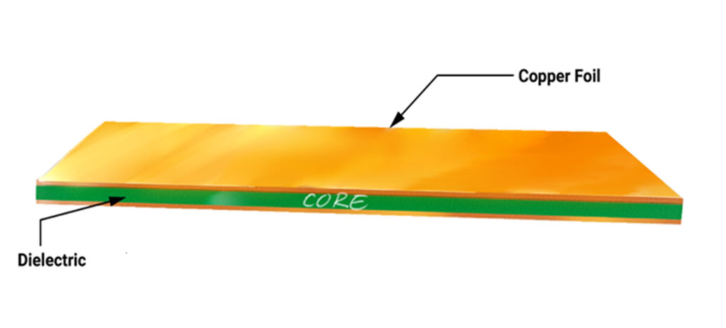
Copper-clad laminates, also known as cores, are made of prepregs and copper foils that have been laminated and cured. Plies of prepregs bonded together form a core. This core is bounded with copper foil on either side to form a copper-clad laminate.

PCB Material Design Guide
9 Chapters - 30 Pages - 40 Minute ReadWhat's Inside:
- Basic properties of the dielectric material to be considered
- Signal loss in PCB substrates
- Copper foil selection
- Key considerations for choosing PCB materials
Download Now
Why are copper conductors better than aluminum?
Copper is well known for its ductility and electrical conductivity. The metal also offers great tensile strength and better thermal conductivity/expansion properties when compared to aluminum. Below are a few reasons to choose copper as a conductor over aluminum in circuit boards.
- Copper offers significantly lower specific electric resistivity and coefficient of thermal expansion over aluminum.
- It is more resistant to corrosion as it reacts less with water when compared to other metals.
- It is one of the easiest metals to solder.
- It is available in lower cross-sections such as 0.5 mils.
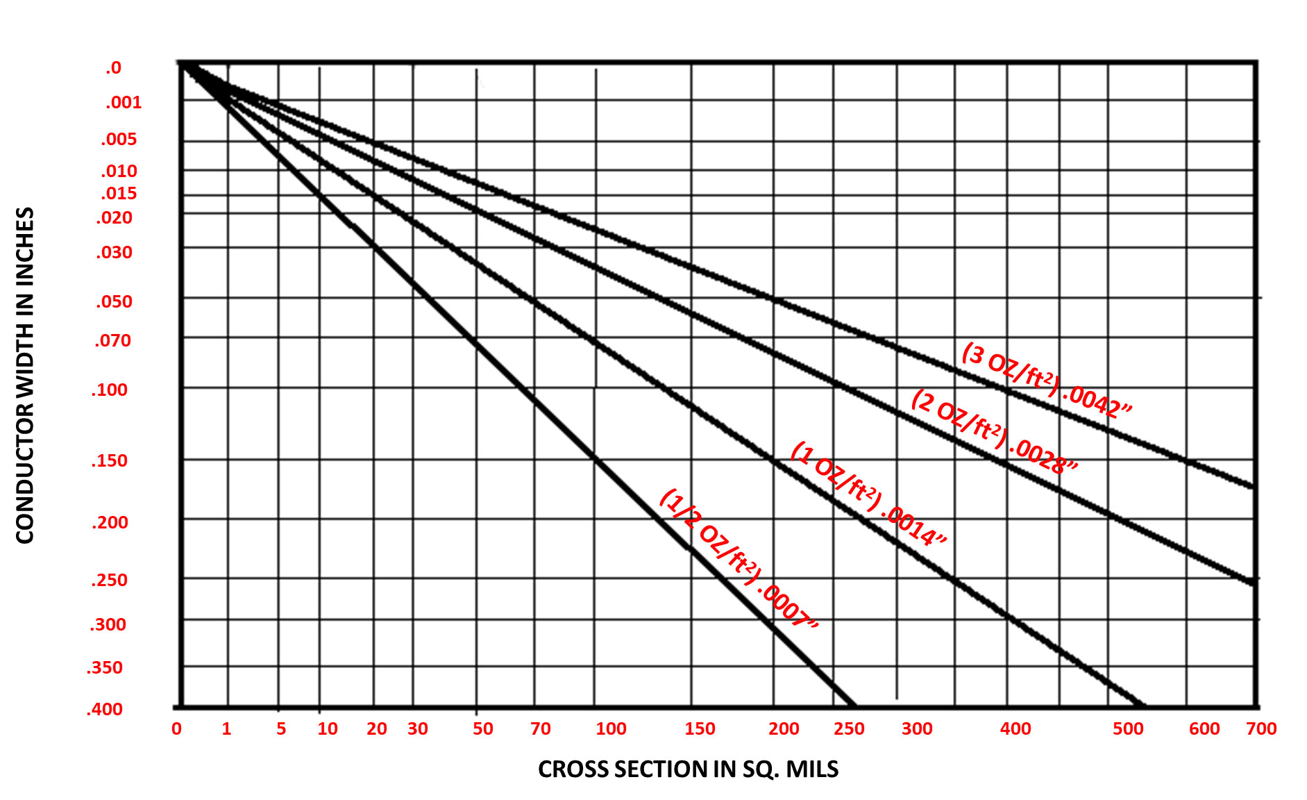
Copper weight and thickness in PCBs
The thickness of the copper on circuits is expressed in terms of ounces. A question arises, why use the unit of weight to specify a thickness? If 1oz (28.35 grams) of copper is flattened to cover 1 square foot of surface area (0.093 square meters), the resulting thickness will be 1.4 mils. Copper weight is measured in ounces per square foot (oz/ft²). The below table shows copper weight versus copper thickness in mils.
| Copper weight | Approximate thickness in mils |
|---|---|
| 1 oz | 1.4 mils |
| 2 oz | 2.8 mils |
| 3 oz | 4.2 mils |
| 4 oz | 5.6 mils |
Current carrying capacity of traces
According to the IPC-2221 generic standard, circuit board trace current limits can be classified further into internal and external layers/conductors. The graphs given below show the relationship between different variables related to trace width. The variables are trace cross-sectional area, temperature rise, and maximum current carrying capacity for external conductors and internal conductors.
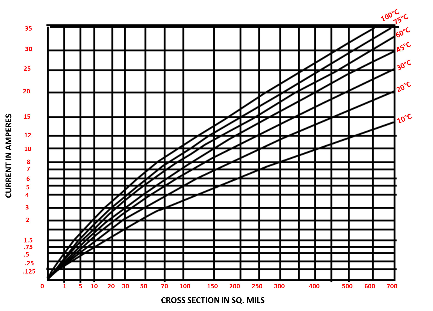
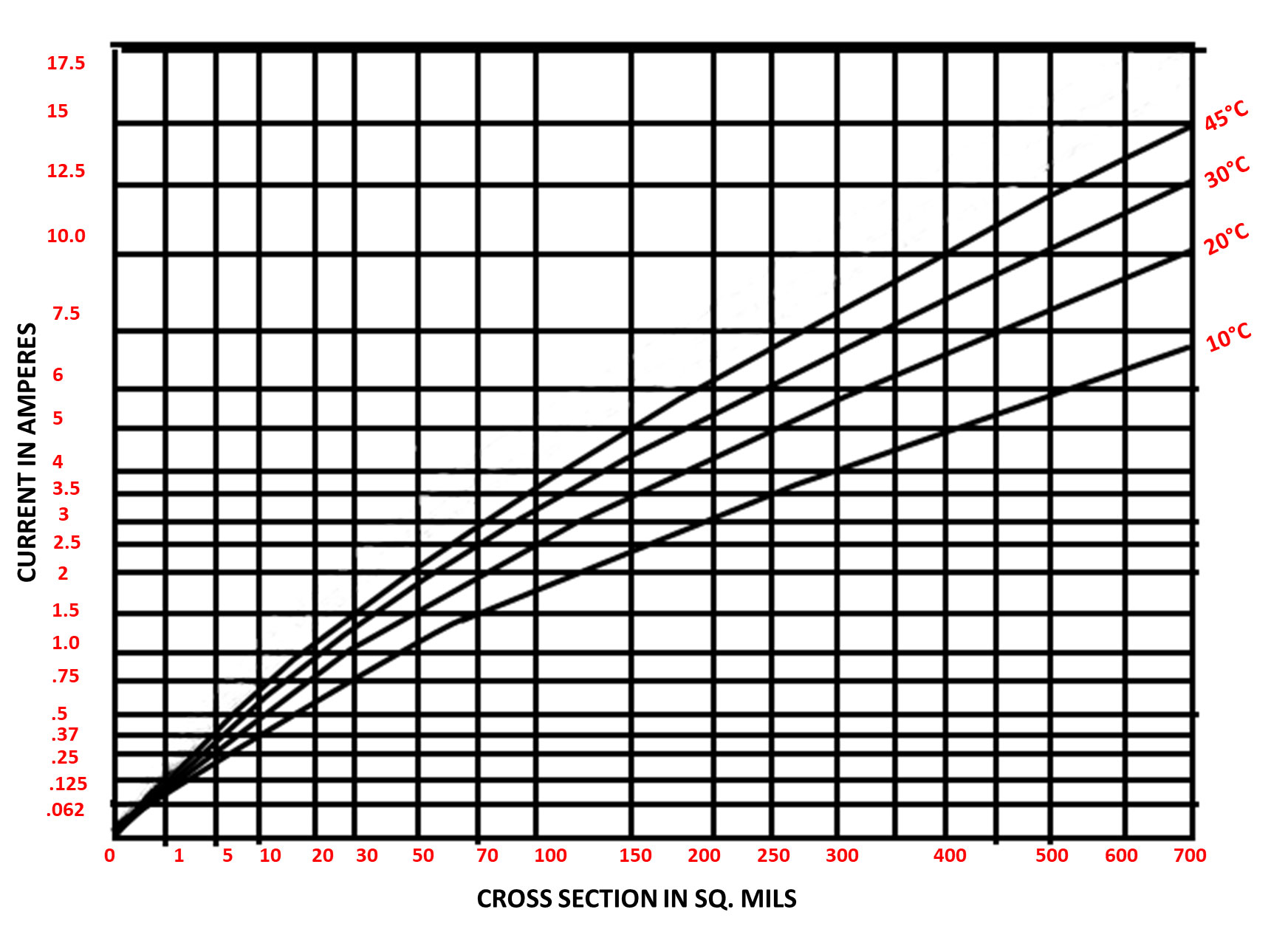
Below is the formula to calculate current carrying capacity of a copper trace.
I = K (ΔT)(0.44) A (0.75)
K = 0.024 for internal conductors and 0.048 for external conductors
ΔT = Maximum temperature difference in °C
A = Cross-sectional area of copper trace in mil²
I = Current carrying capacity in amperes
Copper foil types
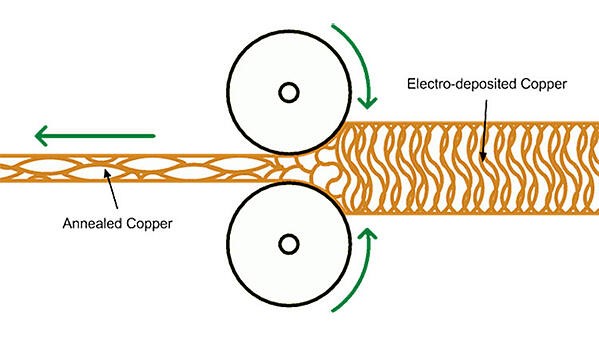
Electro-deposited copper: This type of copper has a vertical grain structure and a rougher surface. Electro-deposited copper is typically used in rigid PCBs.
Rolled copper: A type of copper, made very thin by processing between heavy rollers, extensively used to produce flexible and high-speed boards. Rolled copper has a horizontal grain structure and a smoother surface which makes them ideal for rigid-flex and flex circuit boards.
Copper foil selection
Copper foil selection typically depends on required copper thickness, copper purity, and copper-dielectric interface profile.
Copper thickness: Typical thickness varies from 0.25 oz (0.3 mils) to 5 oz (7 mils). The copper thickness varies as per the application. For example, a higher copper thickness is more suitable for high-power applications.
Copper purity: It is the percentage of copper found in a copper foil. Electronic grade copper foil has a purity of around 99.7%.
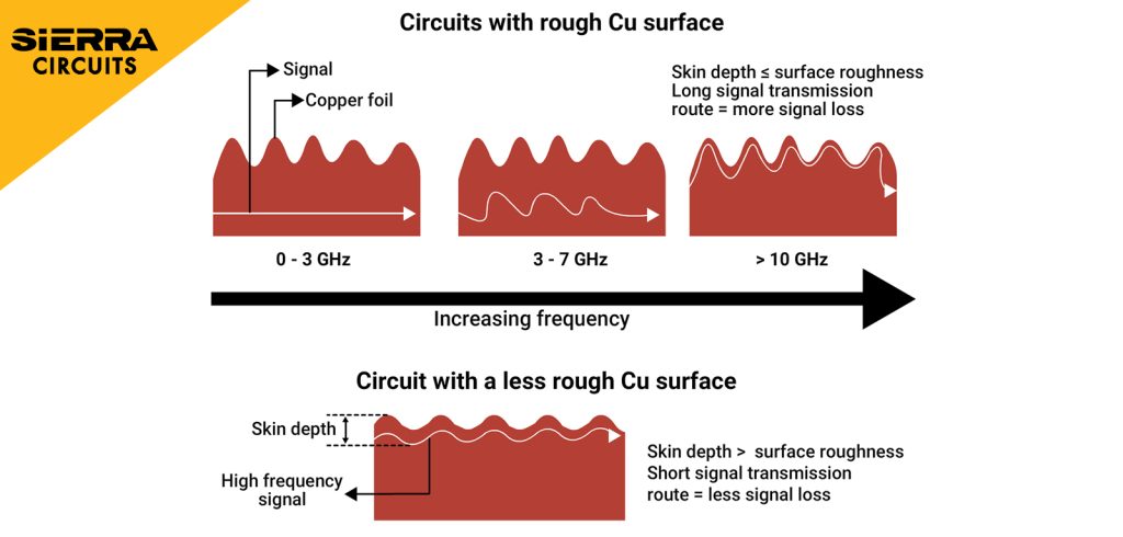
Copper-dielectric interface profile: Low-profile copper has lower signal losses at high frequencies. Hence, it is recommended to choose low-profile copper for high-frequency applications. Here’s a quick infographic that shows the effect of copper profiles on signal transmission.