How is the price calculated for a PCB?
When you’re building a circuit board, it is very important to consider the factors that impact the overall price of the design. The cost structure mainly depends on the parameters such as dielectric materials, number of layers, physical dimensions, and trace parameters.
Circuit board materials
The materials used in the fabrication process will always affect the overall cost of the board. Standard PCBs are laminated using FR-4 substrates. Boards implemented in high-reliable applications such as aerospace and medical equipment require higher-grade laminates. To summarize, high-frequency and high-temperature applications call for dielectrics with extremely good thermal and electrical properties.
Factors that impact material selection
Consider the following characteristics before choosing a material for your design.
- Thermal reliability
- Mechanical reliability
- Electrical stability
- Chemical reliability
High-Speed Material Design Guide
6 Chapters - 19 Pages - 30 Minute ReadWhat's Inside:
- Importance of choosing the right material for your high-speed design
- Parameters that affect material selection
- Effect of dielectric constituents on your circuit board
- Characteristics of high-speed materials
- Effect of resin content and glass weave structure on your PCB
Download Now
Number of layers
The number of layers in your stack-up is also an important cost driver. The PCB price goes up as the layer count increases. The lamination process becomes complicated by adding more layers to your build-up.
The below table gives an estimate of the price increase as the layer count increases.
| Increase in layer count | Increase in overall cost |
|---|---|
| 1 layer to 2 layers | 35 to 40% |
| 2 layer to 4 layers | 35 to 40% |
| 4 layer to 6 layers | 30 to 40% |
| 6 layer to 8 layers | 30 to 35% |
| 8 layer to 10 layers | 20 to 30% |
| 10 layer to 12 layers | 20 to 30% |
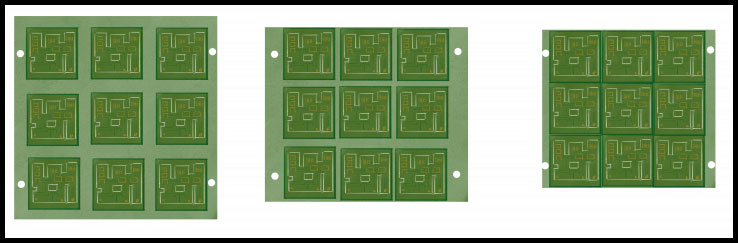
Board outlines
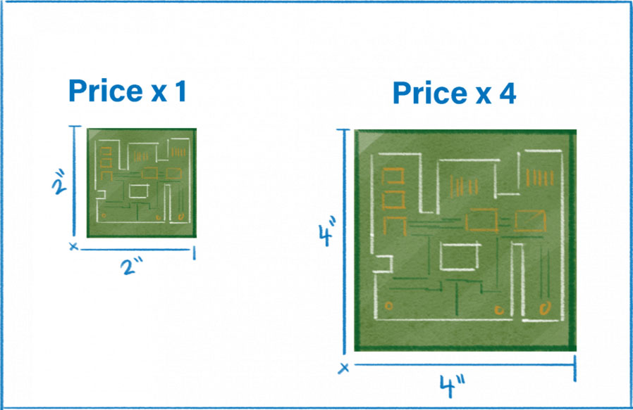
The shape and size (board outlines) of a circuit board should be determined during the early stage of the design. Bigger the surface area, the more expensive it is. When multiple boards are fabricated in a panel, the boards should be placed close to each other for effective usage of real estate.
Trace width and spacing
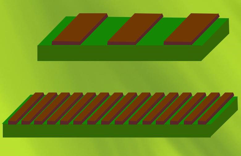
Optimum trace width and spacing are essential to transmit signals without reflections and EMI. The more confined your trace/space is, the more difficult it will be to reliably etch traces and pads. This, in turn, will increase the price of the board.
The thickness of the copper foil
In general, the thinner copper layer boards are less expensive. When thick copper layers are implemented on the inner layers, a higher number of prepregs are required during lamination to fill in the gaps between the copper sections. The circuit board price rises when there is more than ½ oz of copper on the inner layers and more than 1 oz of finished copper on the outer layer. If you utilize very thin copper (less than ¼ oz), you will incur additional costs due to the high cost of processing very thin copper.
Drill holes
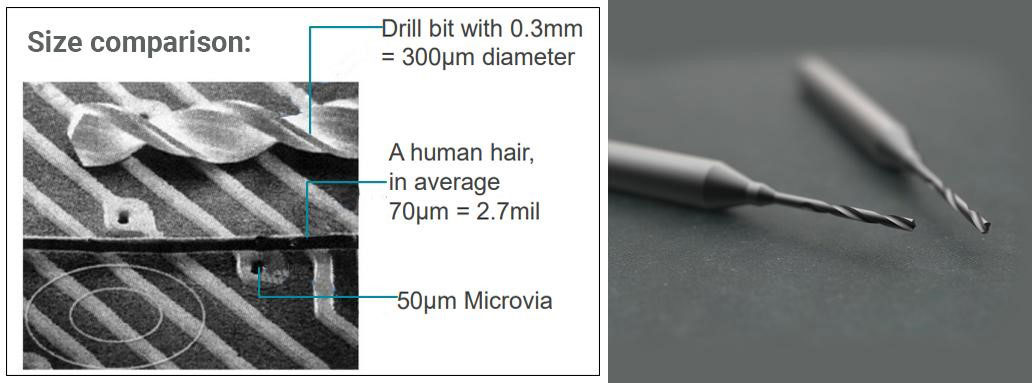
Size of drill holes
Drilling smaller holes demand smaller drill bits, which are expensive when compared to drill bits with a larger diameter. If a hole smaller than 6 mils is required, it should be laser drilled which adds to the cost.
The standard drill bit is 8 mil in diameter, while the advanced drill bit is 5 mil. Small hole size and thick PCB (high aspect ratio) lengthen the duration of drilling, resulting in greater costs.
Drill to copper
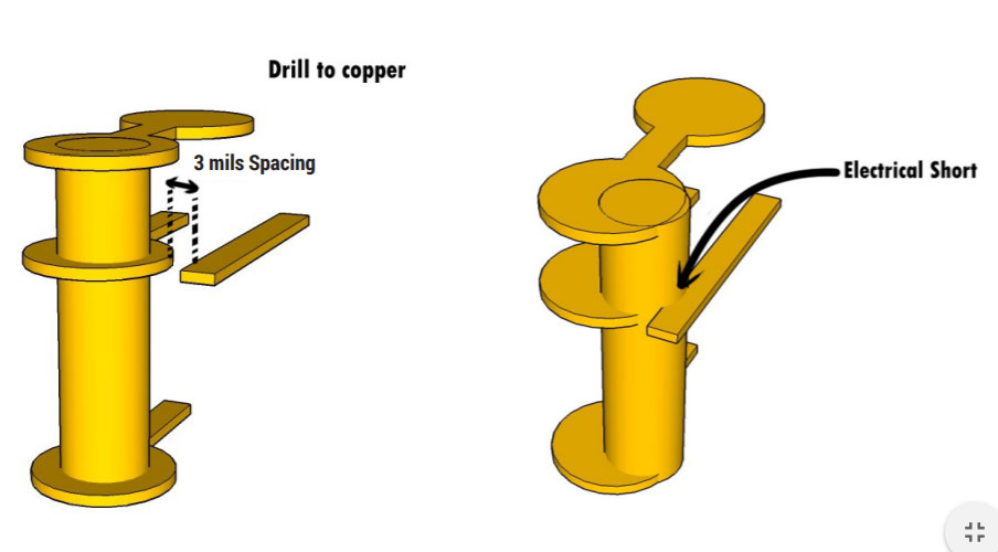
The distance between the edge of the drilled hole and the nearest copper feature on a copper layer is known as a drill to copper (pad, pour, trace, etc.). The smaller the drill to copper, the more expensive the PCB manufacturing process is. Check the manufacturing tolerances here.
Back drilling
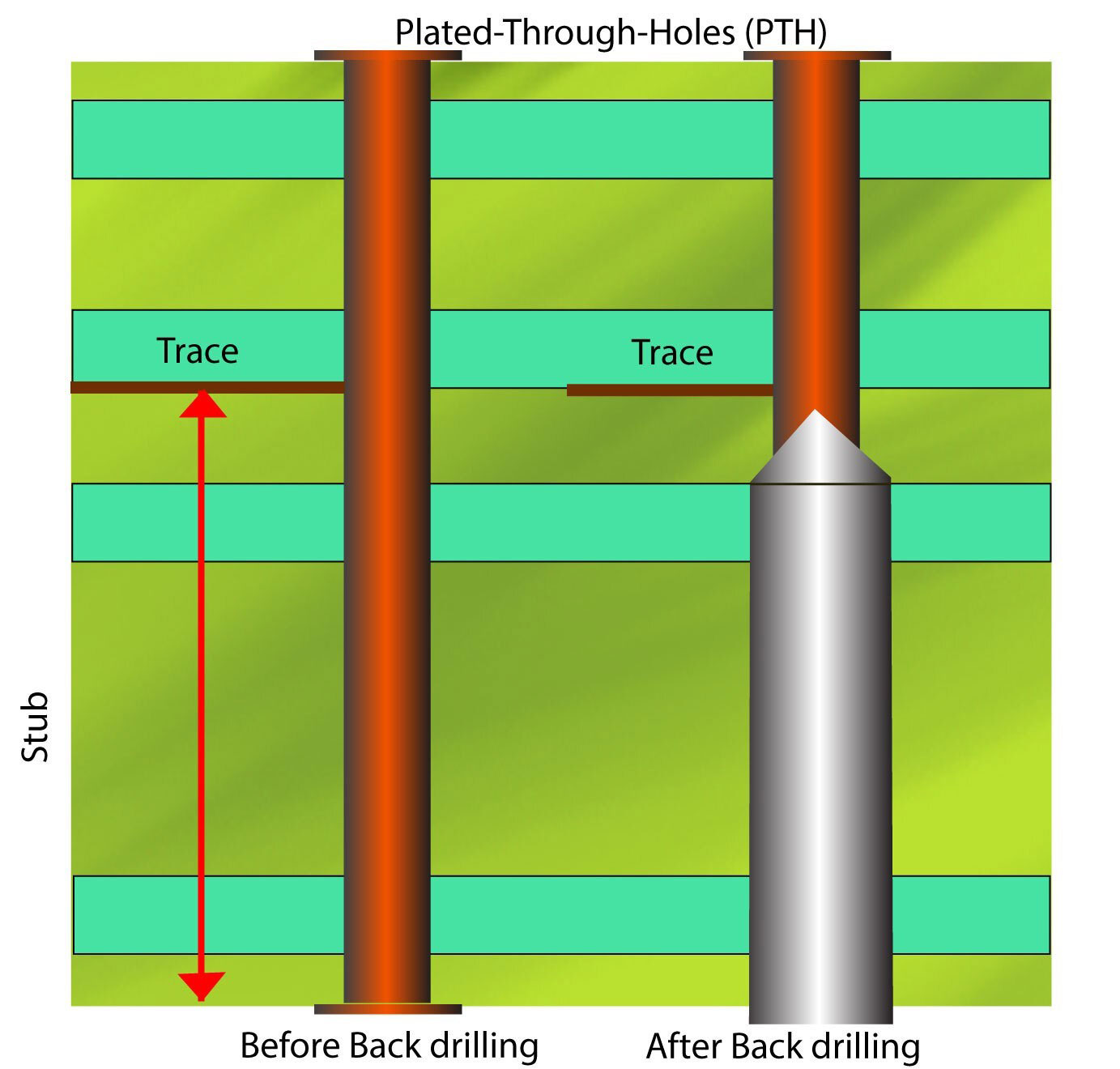
Back drilling removes the conductive via stub by drilling a hole slightly wider in diameter than the PTH. The via stub left after back drilling should be less than 10 mils. This process adds to the overall board’s cost. It should also be noted that back drilling also comes with numerous advantages such as reduced via to via crosstalk, increased data rates, and less signal attenuation with improved impedance matching.
Laser drilling
Laser drilling is a non-contact procedure in which the workpiece and tool do not come in contact. Drill depth may be easily controlled here. A minimum hole diameter of 2 mils (0.002”) can be accurately drilled. Generally, laser drilling costs more than mechanical drilling.
The complexity of your design
The overall price of the board also depends on the manufacturing techniques followed. The cost increases if a complex manufacturing technology is adopted. For instance, while fabricating HDI boards, sequential lamination is used to incorporate microvias into them. This increases the overall cost and the time required to manufacture.
How to reduce your PCB cost?
In this section, let’s have a look at the three primary areas where the overall PCB price can be reduced.
Board design and layout
- Ensure that each section of the design is evaluated and signed off. This reduces unnecessary board respins.
- Have a well-developed design library so you don’t have to keep reconstructing the same parts.
- Design files should be backed up and safeguarded in the event of data loss.
Circuit board fabrication
- Examine the board materials you intend to use. Check if there are any less expensive options. In many circumstances, basic FR-4 will suffice instead of an expensive dielectric material.
- Try to keep the number of layers as low as possible. However, it should also be noted that a higher layer count may be required for improved signal integrity and overall board performance. In this situation, a small cost increase may end up saving you more money.
Design for manufacturability
- Make sure the layout is optimized for soldering operations. What may be ideal for wave soldering may pose issues during solder reflow. These kinds of errors can lead to unforeseen rework costs.
- Ensure that your component arrangement provides adequate room on the board for debugging and rework.
- Automated optical inspection (AOI) should be performed to ensure that the board is assembled correctly. If the board is not designed for AOI, then the manufacturer will have to test the board manually.
Always collaborate with your CM during the early phase of the design. This can reduce the PCB price and cut down the time required to fabricate and assemble your circuit boards.


