High-frequency circuits feature higher integration and higher routing density. Layouts for these kinds of designs can be developed by adapting better termination schemes and routing guidelines.
What are high-frequency PCBs?
Any PCB that operates at a frequency of 100MHz or above can be considered a high-frequency PCB. The laminate materials used to manufacture such boards feature low dielectric constant, high CTE, low loss tangent, and advanced composites. These boards are used in military, medical, and advanced communication applications such as GPS, radar, and base stations.
High-frequency PCB design checklist
- Use less number of vias: Vias introduce a distribution capacitance of about 0.5 pF. Reducing the number of vias can increase the signal speed and reduce the possibility of data error. Via stubs add impedance discontinuities, resulting in signal integrity problems.
- Implement shorter leads between the pins in a high-frequency circuit: The radiation intensity of the signal is directly related to the routing length of the signal line. Longer high-frequency signals lead result in increased coupling with other components. That is why a shorter routing length is preferred for clock signals, DDR, USB, Gigabit, and HDMI.
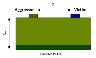
- Avoid crosstalk: The parameters of PCB layers, the spacing of signal lines, the electrical characteristics of the source and load terminals, and the signal line connection mode affect crosstalk. To avoid crosstalk, follow the below-mentioned layout techniques:
- Isolate signal lines by inserting a ground plane.
-
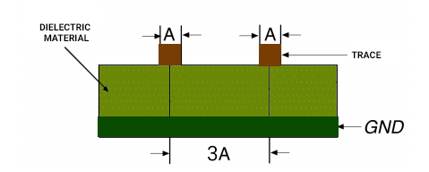
- Add more spacing between adjacent signal lines and minimize the parallel length of signal lines. Use at least 3W spacing between traces, where W is the width of the trace.
-
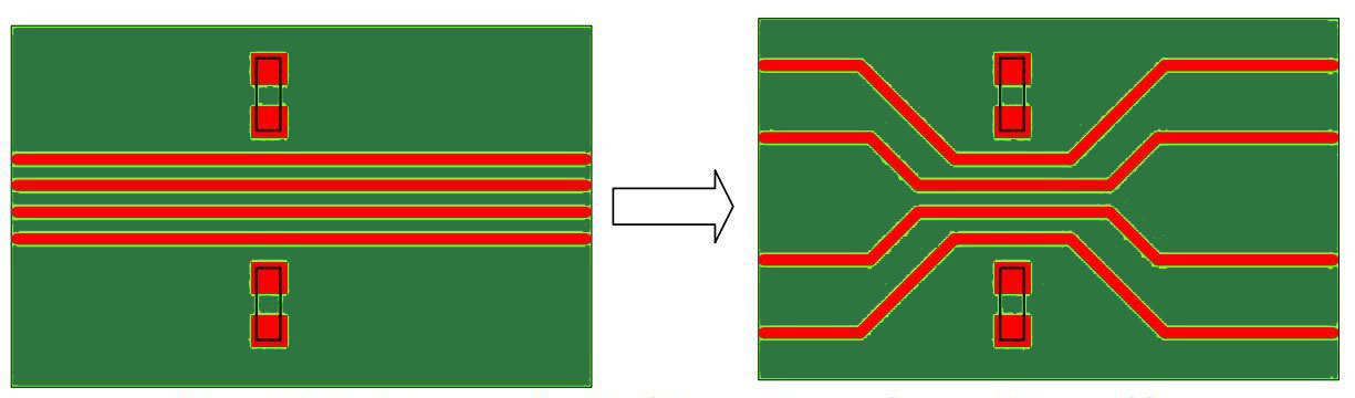
- Route clock line in a perpendicular fashion to the signal lines rather than parallel.
- It is not possible to avoid parallel lines in the same layer, but they can be routed perpendicularly to each other in the adjacent layers.
- Surround clock lines in between two ground lines and incorporate ground stitching vias to reduce the parasitic capacitance and, hence, the crosstalk.
- The low-voltage differential clock signal should be directed as far as possible from the high-frequency clock signal. Give proper attention to perforation integrity.
- Maintain center-to-center separation between two traces at least three times their width.
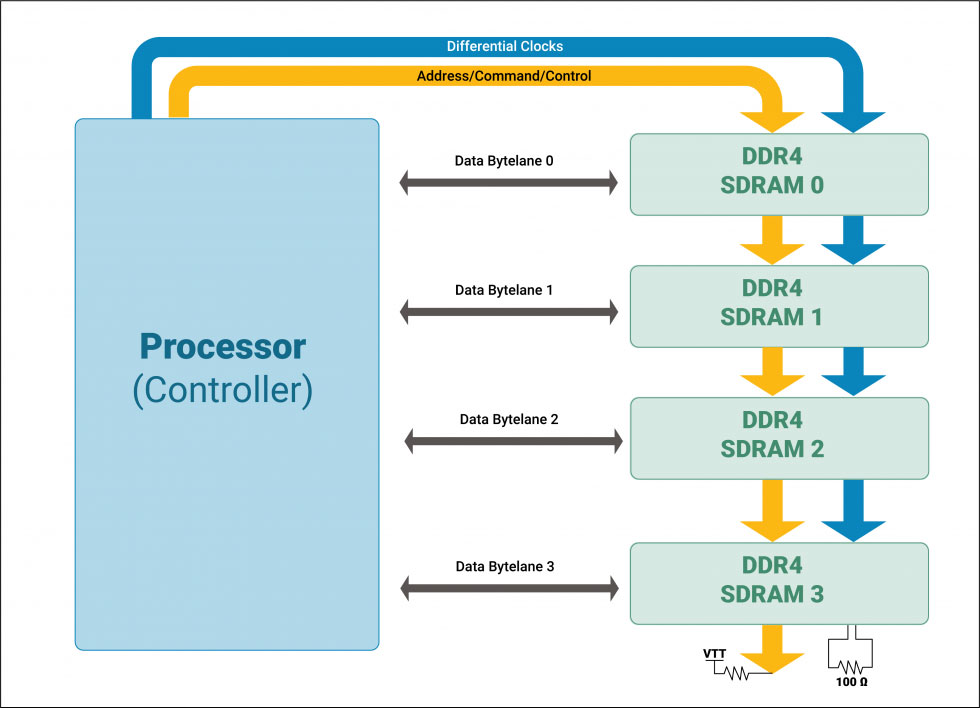
- Adopt fly-by topology/ daisy chain routing in DDR4: This routing technique reduces the reflections during high-speed data transfer. It also reduces the number and length of the stubs, hence improving the signal integrity and timing on loaded signals.
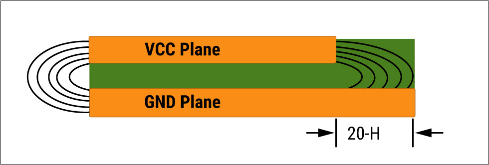
- Use the 20H rule to reduce plane coupling: Make the power plane 20 times smaller than the dielectric thickness between the adjacent power and ground planes. It will allow any fringing to be absorbed into the ground plane instead of radiating it externally.
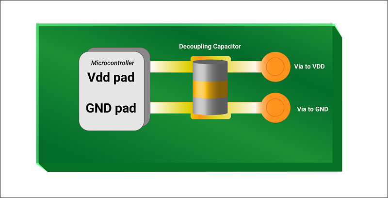
- Add decoupling capacitance as near as possible to the supply and ground pins: It inhibits the interference of high-frequency harmonics on the power supply pin.
- Keep loop area as small as possible: High-frequency signals should not form a loop when wiring. If it is there, keep the area as small as possible.
- Take your time to decide the type of transmission line: Opt for a microstrip or stripline trace geometry. Microstrip arrangement only provides one reference plane separated by a dielectric. If you need more shielding, go for a stripline arrangement between multiple ground planes and a dielectric.
- Maintain accurate impedance matching: When the impedance does not match, the signal will suffer reflections in the transmission channel, resulting in ringing, overshoot, and undershoot.
- Select low profile copper-dielectric interface: Low profile copper-dielectric interface has lower signal copper losses at high frequencies.
- Do not use FR4 for high-frequency applications: FR4 exhibits high dielectric loss and steeper Dk versus frequency response curve at high frequency. You can try our material selector tool, to pick the right one.
- Adopt orthogonal routing while directing a signal on different PCB layers.
- Always check the highest frequency net and evaluate the fastest rise time in the system.
- Check the electrical specifications at the inputs and outputs of the sinks and sources.

Signal Integrity eBook
6 Chapters - 53 Pages - 60 Minute ReadWhat's Inside:
- Impedance discontinuities
- Crosstalk
- Reflections, ringing, overshoot and undershoot
- Via stubs
Download Now
What are the typical materials used for high-frequency boards?
The following materials are suitable for a high-frequency PCB manufacturing process:
- Materials, namely, Isola I-speed, Isola Astra, and Tachyon exhibit low loss at high frequencies.
- Rogers 4350B and Panasonic Megtron 6
- Rogers 4350B showcases low loss and is suitable in the frequency range of 500MHz to 3GHz.
- Panasonic Megtron 6 also showcases low loss and is suitable in the frequency range of 3GHz and above.
When signal speed increases, the high-frequency effect leads to ringing, crosstalk, reflections, ground bounce, and impedance mismatch problems. It not only affects the digital properties of the system but the analog properties also. These issues can be eradicated using strict design tactics or adopting accurate layout guidelines. Signal routing, termination methods, and power distribution techniques can help the designers to realize a fruitful high-frequency circuit board.


