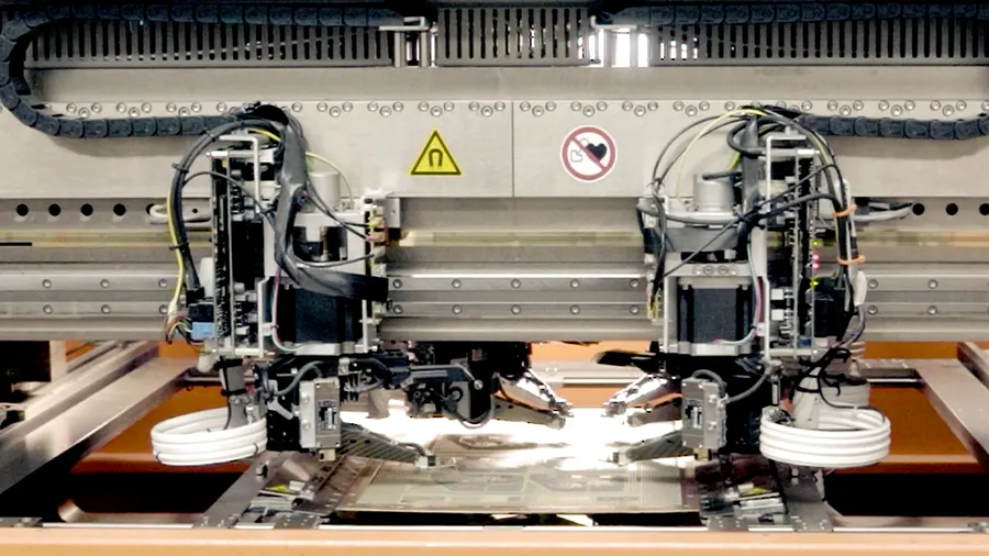
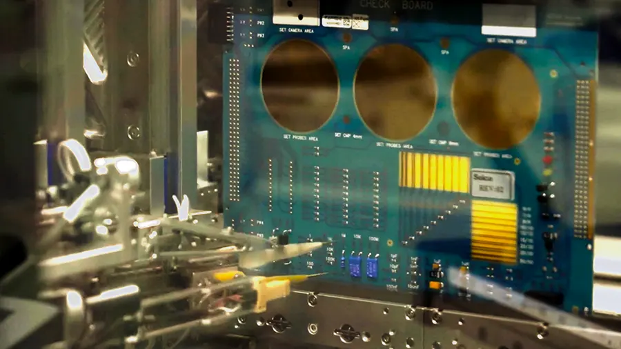
What comes to your mind when we talk about a PCB? Motherboard of your computer, a not so simple green board? A board looking like that maze game of yours? Or may be a city plan? No matter how it seems to you, it’s everywhere, literally everywhere. It is the heart of modern electronics. Its evolving and changing the way we see the electronics world every day. And we are a proud part of this dawn of a new era!
The Evolution of PCBs
Before the existence of PCBs, it was all about point-to-point construction. The first PCB concept hit the intellectual world in the 1920s, with countless possibilities. Boards back then were made out of Bakelite, Masonite or plain pieces of wood. The first double-sided PCB with plated through-holes was introduced in 1947. By the 1950s to 1960s, resins and other materials were incorporated in circuit boards. PCBs of this generation were printed only on one side with electrical components on the other side. The year 1956 was a big step forward for the industry. A patent was granted to a group of U.S. Army scientists for the process of assembling boards. The first multi-layer PCBs were produced in 1960. 1970s featured smaller PCBs, thanks to the introduction of the hot air soldering method. During the 1980s, SMT replaced through-holes wherever they could, making the PCBs smaller and faster. The use of multi-layered PCBs in the 1990s lowered the cost of production.
From wood pieces to modern smart-looking green boards, PCBs have evolved in terms of everything. Earlier, they were only associated with computers. But now with microelectronics, almost everything is drowned in PCB. Almost all types of consumer electronics like TV, radios, digital cameras and cell phones.
Apart from that PCBs are everywhere, be that in industry machinery like motor controllers, industry load testers. Or in automotive and aerospace industries to medical devices and wearables. Even lightings in several places uses PCBs nowadays.
