There is an ongoing trend shift in surface finish technology from HASL towards alternative finishes such as ENIG, immersion tin, immersion silver, and OSP (organic solderability preservative). This shift is caused by environmental concerns due to the use of lead in electronic assemblies. Immersion tin or white tin is one of the lead-free alternatives currently present in the electronics industry.
What is immersion tin or white tin?
Immersion tin is a coating of tin deposited on the copper layer of a PCB using an electroless chemical process. The layer of tin protects the circuit board from oxidation, thus increasing its shelf life. It usually appears as white after the plating process, hence known as white tin. This is the most economical method out of all the immersion methods.

Why is immersion tin used?
- Immersion tin is a lead-free surface finish, which is highly desirable in today’s age.
- This is the ultimate surface finish for fine pitch surface mount components due to its ability to give a flat, thin, and smooth surface for PCB assembly.
- This process is highly feasible. Moreover, it requires less amount of water and chemicals for the application process.
- It supports any kind of rework due to defects that occur while soldering components.
Thickness specifications of immersion tin
As per IPC-4554 standard, the typical value of immersion tin thickness ranges from 1.15 µm (46 µin) to 1.3 µm (52 µin).

IPC Class 3 Design Guide
8 Chapters - 23 Pages - 35 Minute ReadWhat's Inside:
- IPC guidelines for manufacturing defects
- IPC standards for assembly processes
- Common differences between the classes
- IPC documents to set the level of acceptance criteria
Download Now
How to apply immersion tin?
White tin can be applied through the following steps:
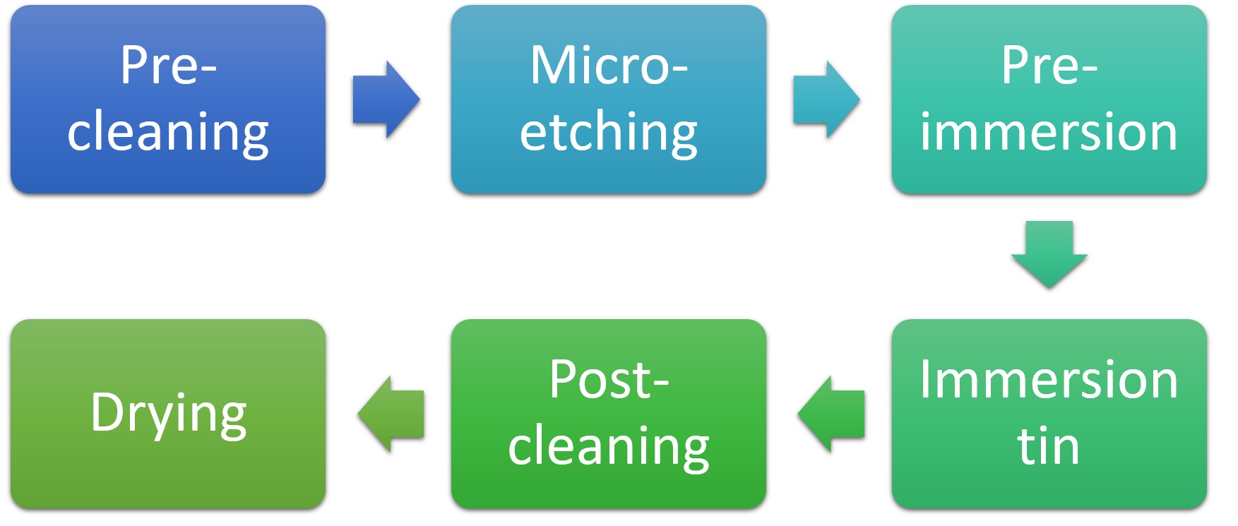
1. Pre-cleaning
This is the first step in the plating process. The circuit board is dipped in an acid solution to remove oil, grease, and other surface impurities. The surface is again washed with water to remove any remaining cleaning solution and surface remnants.
This step increases the efficiency of the plating process.
2. Micro-etching
Here, the board is again dipped in the solution containing sulfuric acid (H2SO4). This acid provides the coarseness to the copper layer structure to prepare it for binding with the tin layer. Again, the surface is washed with water to remove any residues.
3. Pre-immersion
In pre-immersion, the PCB is rinsed with an acid to prevent early oxidation of the copper surface. This offers a good framework for tin deposition.
4. Immersion tin
The circuit board is immersed in a solution consisting of tin cations to accelerate the electroless reduction process. The copper metal is reduced by the tin ions. This develops a thin and flat tin layer on copper pads.
To obtain good results, it is necessary to keep an eye on process parameters as well as chemical composition.
5. Post-cleaning
In this step, the PCB should be cleaned with warm water to remove plating salts and to prevent staining when dried. The board will look dull if rinsed poorly.
6. Drying
It is crucial to dry the board after cleaning. Drying removes moisture content from the surface. It can be done either by clean forced air drying or by a warm oven bake. It is critical to ensure the baking duration and operating temperature of the oven.
Pros and cons of immersion tin or white tin
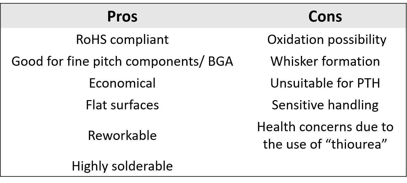
It is recommended to avoid this finish because of poor solderability (due to extended storage), tin whisker formation, and the presence of carcinogenic elements (thiourea). Choose the appropriate surface finish based on the environment in which the board is being used. Surface finish selection is crucial when a PCB is manufactured for specific environments such as defense and space, and medical. Immersion tin or white tin is suitable for HDI boards, BGA, and press-fit applications.


