At low frequencies (<50 MHz), the signals remain within the data characterization limits, and the circuit board performs as intended. When speed increases, impedance mismatching, crosstalk, reflections, ringing, and ground bounce issues are seen due to the effects of higher frequencies. These factors affect not only the digital properties but also the analog characteristics of the system.
These issues are commonly noticed these days due to the increasing data rates for I/O and memory interfaces. Here, you’ll learn 10 high-speed layout design rules to build an efficient circuit board.
What is a high-speed signal?
Signals with frequencies above 50 MHz are considered high-speed signals (clock signals). Ideally, a clock signal is a square wave, but it is practically impossible to change its ‘LOW’ level to a ‘HIGH’ level (and vice versa) instantly. It has a specific rise and fall time, which makes it appear to be a trapezoid in the time domain.
It is worth noting that the amplitude of the clock signal’s higher-frequency harmonics in the frequency domain depends upon its rise and fall time. If the rise time is longer, the magnitude of the harmonics will become smaller.
10 high-speed layout design rules
While designing a circuit board for high-speed applications, strongly focus on the layout. The design rules mentioned below will help you maintain signal integrity and also reduce the manufacturing cost.
1. Have a common ground plane right below the signal traces
This ensures minimal impedance between any two ground points in the board. The ground plane should never be broken by routing any tracks in it.
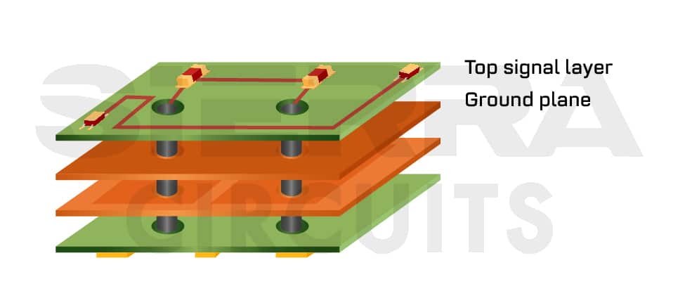
When there is a requirement to route tracks on both sides of a circuit board in the same area, a good ground plane is no longer guaranteed. In this case, the only solution is to implement ground planes on both sides of the traces that are interconnected by plenty of vias.

To learn how to design a high-frequency board, download our e-book.

High-Speed PCB Design Guide
8 Chapters - 115 Pages - 150 Minute ReadWhat's Inside:
- Explanations of signal integrity issues
- Understanding transmission lines and controlled impedance
- Selection process of high-speed PCB materials
- High-speed layout guidelines
Download Now
2. Ensure adequate spacing between vias to avoid hotspots
When the current encounters a via, the flow is disrupted can cause current concentration around them. This may lead to hotspots and hinder the signal transmission.
Always place vias in a well-spaced grid pattern to ensure uniform distribution of current flow within the power/ground plane and mitigate hot spot risks.

3. Place vias symmetrically to eliminate impedance discontinuities
When vias are arranged symmetrically along signal lines, electrical properties such as impedance and signal transmission are more consistent. This symmetry reduces impedance variations caused by asymmetrical via placements, which can lead to signal reflections and degradation.

4. Maintain minimum bends while routing
Excessive bends in trace routing can introduce impedance variations and signal reflections, particularly when dealing with higher frequencies. The wider angle decreases mechanical stress on the PCB material and copper traces, lowering the possibility of fracturing or delamination during manufacturing.
There has been a misconception that using 90° bends when routing traces on a PCB can lead to impedance mismatches. However, this idea is not accurate for most practical applications. In reality, any potential issues with a 90° bend affecting impedance only become significant at extremely high frequencies, typically in the terahertz (THz) range.
5. Add serpentines to length match the traces

When utilizing serpentine traces to achieve length matching, it is essential to carefully consider the placement of serpentine patterns at the root of the length mismatch. This ensures that the positive and negative signal components are propagated synchronously over the connection.
Each segment of a differential pair connection must undergo individual matching. Segments can be divided by connectors, serial coupling capacitors, or vias.
In the image below, the two bends compensate each other, as seen on the left side. However, when vias divides the differential pair into two segments, each bend must be compensated separately. This ensures synchronous propagation of positive and negative signals through the vias.

6. Maintain at least 3W spacing between the signal traces to minimize crosstalk
Ensure optimum spacing between the traces and components. The separation distance between adjacent traces and neighboring components should be as large as possible to eliminate the risk of crosstalk. The general rule is that the separation distance should be equal to three times the trace width.
7. Implement daisy chain routing to avoid long stubs
The long stub traces may act as antennas and radiate inteference and increase problems with EMC. Daisy chain routing connects components in a series, avoiding long branches or stubs. This technique reduces the length of potential antennas, mitigating EMI issues.

8. Do not place components and vias between differential pairs
Avoid components or vias between differential pairs, even if the signals are routed symmetrically. Components and vias create an impedance discontinuity and EMC. Diff pairs are designed to transmit signals with opposite polarity, and any interference between them can result in signal integrity problems such as crosstalk and interference.

9. Design differential pairs with symmetrical paths and keep signals in parallel
Differential pairs should have uniform impedance throughout their length for optimal signal propagation and common-mode noise cancellation. Any asymmetry in routing, including variations in spacing or uneven bends, can disrupt the impedance balance and introduce crosstalk between differential signals. Keeping the traces parallel is, therefore, essential to minimize the risk of unequal coupling and potential noise injection.

10. Route differential signals on the same layer
Always route both traces of a diff pair on the same layer for maintaining a consistent electrical environment and minimizing impedance variations. This approach avoids the potential for signal degradation that can occur when switching layers through vias.

The challenges associated with high-speed board layout become increasingly apparent as frequencies exceed 50 MHz. Issues such as impedance mismatch, crosstalk, reflections, PCB ringing, and ground bounce can significantly impact both digital and analog sections of a circuit.
By adhering to these high-speed layout design rules, you can mitigate the adverse effects of high-speed signals, optimize signal integrity, and ensure electromagnetic compliance.


