Surface mount technology (SMT) components are easily assembled by automated machines, making assembly quicker, faster, and cost-effective.
Pick-and-place equipment is generally used to assemble SMT devices. Such assembly begins with board and component inspection.
What is SMT assembly?
Surface mount technology assembly is a technique in which electrical and electronic components are mounted directly on the surface of a circuit board. Electrical and electronic components that follow this mounting technique are known as surface mount devices (SMD). This technology minimizes fabrication costs and increases efficiency.
What is the difference between SMT and SMD?
An SMD is a leadless electronic component that is mounted on a PCB directly without drilling holes. And SMT refers to the process (technology) used to mount SMD components on a circuit board.
To learn learn more, check different SMD component package sizes.
Benefits of surface mount technology
A few benefits of using SMT for board design include:
- More compact board design as components can be placed closer together. This enables higher circuit speeds.
- Production setup is faster compared to through-hole technology (THT).
- Minimizes production cost since drilling isn’t required.
- SMD components can be mounted on both sides of the board.
- Better EMC performance due to lower lead inductance.
- Provides enhanced high-frequency performance as the undesired effects of RF signals are mitigated.
For more details, see the advantages and disadvantages of SMT.
Drying conditions for BGA and PCB
The storage temperature for BGA devices that are temperature-sensitive is between 20 – 25°C with a relative humidity (RH)of 10%. Once BGA packages are opened, they must be used within 8 hours under the operating environment conditions of ≤30°C/60% RH. To prepare BGA devices for soldering, they are baked at 125°C to remove any moisture content.
The circuit board drying temperature for dehumidification is <60°C (low-temperature heat), and the water vapor content in the atmosphere should be <0.05g/m3.
Board preparation
The following steps are implemented for board preparation:
- Solder paste application: Solder stencils designed from the PCB CAD output files are used to apply solder paste to the SMT pads present on the board. This paste is stored in a cool and controlled environment. Once the solder paste is applied, the circuit boards should be sent for assembly within a specified time.
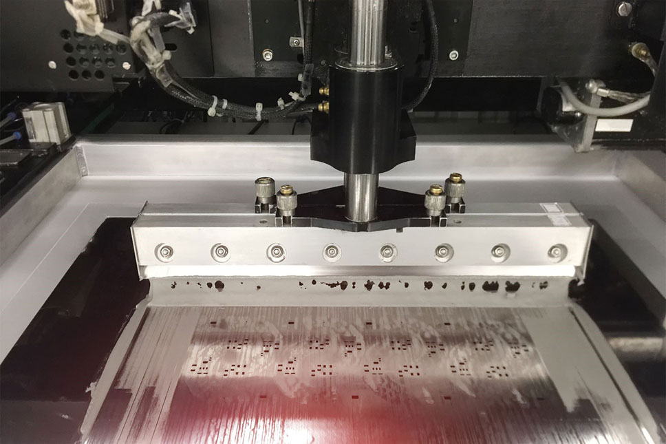
- Solder paste inspection: After paste application, the PCBs are subjected to solder paste inspection (SPI), similar to AOI tools used post assembly. SPI analyzes the location of the paste, paste volume, and other parameters.

PCB Design for Assembly Handbook
6 Chapters - 50 Pages - 70 Minute ReadWhat's Inside:
- Recommended layout for components
- Common PCB assembly defects
- Factors that impact the cost of the PCB assembly, including:
- Component packages
- Board assembly volumes
Download Now
Component preparation
Like circuit boards, components are also prepared for assembly by classifying them into kits. This process is as follows:
- Bill of materials (BOM) for assembly kits: The manufacturer will take the BOM data and the related barcodes for the part to generate the assembly kit BOM.
- Kits are stocked with components: The required parts are retrieved from stock and
added to the assembly kit. After the kits are prepared, they are sent to the pick-and-place machines in the production line. Read kitting guidelines for assembly to understand kit criteria and more.
After loading the right components in the cartridges, programming the pick-and-place machine with the placement data, and solder paste application on the boards, the SMT assembly kicks off.
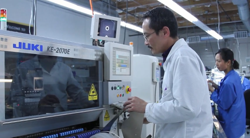
- Components are prepared for placement: Pick-and-place machines have cartridges to hold different types of components for assembly. Parts are loaded from such cartridges as required during the assembly process. To ensure the right cartridge is matched to the corresponding assembly kit BOM, every cartridge will have its distinct key.
- Reflow soldering
- Inspection (AOI, X-ray, and/or visual inspection)
This process is repeated for the secondary side in case the circuit board has components on both sides.
Unsuited components for pick-and-place machines
While a majority of components can be placed using pick-and-place machines, some of them can only be assembled manually. The reasons for this are stated below:
- Thermal stress: Certain components might have high sensitivity to heat, making them unsuitable for moving through the solder reflow oven.
- Robust solder joints: Parts such as connector leads require a relatively more robust solder joint.
- Panelization separation: Panelization subjects components to significant amounts of mechanical stress that might damage them. The part, in this case, will be placed after panel separation.
- Too light: Certain parts are not heavy enough for an adequate mass-to-adherence ratio during automated surface mount assembly.
The key to efficient PCB assembly is accurate placement and assembly of SMT components. As a designer, you should also be aware of common errors that occur in SMT.


