Contents

On-demand webinar
How Good is My Shield? An Introduction to Transfer Impedance and Shielding Effectiveness
by Karen Burnham
While manufacturing a PCB, controlled impedance can be achieved through specific dielectric thickness and by providing the target ohms on each layer. The factors that influence impedance are the PCB materials’ dielectric, the trace thickness, width, and height from the ground plane.
The designer should make sure that the manufacturer has the ability to provide the right pattern size, position, and tolerance. The board might turn out to be useless if these parameters aren’t achieved.
In this post, we will take you through the following key aspects that require due attention while fabricating a controlled impedance PCB:
Manufacturing controlled impedance PCBs
The impedance of traces is defined by a number of parameters, which include trace width (W), the thickness of the trace (T), the height of the trace (H) from the ground plane, and the dielectric of the PCB material. When you define a trace as a controlled impedance trace, the impedance matters more than the size of the copper feature for PCB manufacturers. So, they might alter certain specifications that was provided by you, such as the trace width, the trace height, and the dielectric thickness. However, they will make sure that the final impedance is within the tolerance. The following aspects need clarity while manufacturing controlled impedance PCBs.
Also read, How to Build a Flex Stack-Up with Controlled Impedance
# Specify a controlled dielectric board in place of controlled impedance
You can get controlled impedance in two ways: first is to specify the dielectric thicknesses that you are looking for in your fabrication drawing and not specify any of the controlled impedance parameters at all. The second method, which we think is the better way is to specify the layers in which you’d like your impedance lines on and the target ohms. Standard tolerance is plus or minus 10% ohms. If tighter tolerance is needed, we can deliver plus or minus 5% ohms. Tighter tolerance would require a different game plan ahead of time. Example fabrication notes can be found in our controlled impedance design guide.

Controlled Impedance Design Guide
6 Chapters - 56 Pages - 60 Minute ReadWhat's Inside:
- Understanding why controlled impedance is necessary
- Stack-up design guidelines
- How to design for impedance
- Common mistakes to avoid
Download Now
Controlled dielectric thickness: The designer provides the controlled dielectric stackup to the manufacturer. Since impedance traces are not specified here, the manufacturing focus is completely upon building a board within +/-10% tolerance of the specified dielectric thickness from layer to layer.
Impedance control: Here, the impedance is controlled through the dielectric thickness, the trace width, and space. The manufacturer performs a test to ensure that the desired impedance can be achieved using TDR coupons. Some adjustments are made depending upon results from the first articles to meet the designer’s needs, and the boards are manufactured within the specified tolerance.

# Press-Out thickness for manufacturing controlled impedance PCBs
Remember, we also plan based on the press-out thicknesses that we expect from the prepreg. This is based on the amount of resin in the prepreg and the copper area and thickness of copper on the opposing layers. We get the copper area from the data you send us to create a final model. So, we don’t follow the thickness on the datasheet. We follow our press-out thicknesses in modeling, which varies slightly from design to design. That is why, after an initial stackup and target line widths, we come back to you for approval on small adjustments to the trace widths and spacing.
# The difference between core and prepreg
A multilayer PCB manufacturing requires two forms of PCB materials: cores and prepregs. Cores are copper clad PCB laminates. Their dielectric thickness does not vary after lamination because they are fully-cured materials (copper is on the outside). Prepregs are semi-cured materials, and they are used as a bonding material between two core laminates. After lamination, the final thickness of a prepreg material depends on the percentage of the copper in the adjoining conducting layers, the height of the copper in these layers, and the type of the prepreg used. All semi-cured prepregs are turned into fully-cured dielectric after the lamination process.
It is crucial that during the lamination process, a high degree of process control and integrity is maintained so that post-lamination thicknesses are reasonably predictable, and the mechanical integrity of copper conductors is maintained. All of Sierra Circuits’ lamination cycles have computer-controlled profiles to achieve consistency. Click why controlled impedance really matters to learn the design aspects of controlled impedance PCBs.
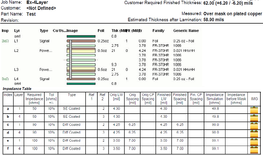
Let us take an example of a 0.062-inch (62 mils) thick PCB stackup:
The figure below shows a 4-layer stackup consisting of two cores and three prepreg layers. L2 and L3 are single-sided copper cores, and three plies of 1086 type prepreg (usually indicated by 3 x 1086 in the stackup diagram) are sandwiched between them. L1 and L4 are outer layers made up of copper foils with 1 x 1086 prepreg between L1-L2 and L3-L4.
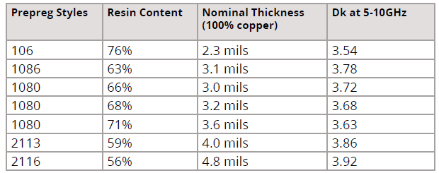
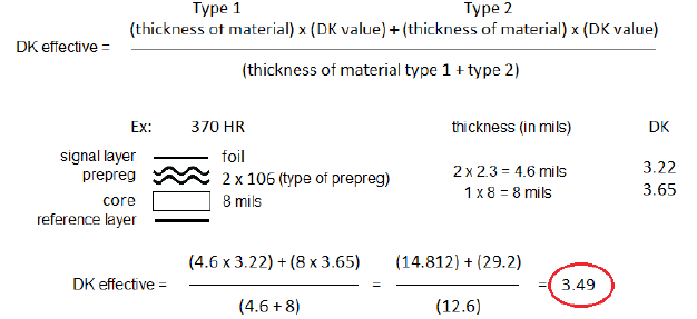
A critical component of the PCB material is the resin content. The percentage of the resin content greatly affects the final thickness and the dielectric constant. The higher is the thickness, the lower is the dielectric constant of the PCB material. For the same type of PCB material, different thickness cores (PCB laminates) and different types of prepregs have different resin contents, therefore different dielectric constants. When PCB manufacturers model the impedance traces, they take care of such fine variations in dielectric constants due to resin content. Read more on how to choose PCB materials and laminates for fabrication.
The thickness and the dielectric constant of the generic prepreg glass styles for Isola 370HR material are given below:
# Core vs. foil construction
Some customers, however, choose to go with a core construction over a foil construction. The core construction is when we use an already cured core of material for the outer layer and the next layer so that the dielectric thickness does not change after lamination. This construction takes away the variation in dielectric height. However, this type of construction or stackup is not always possible, like in HDI PCB manufacturing.

# Controlled impedance and HDI PCBs
All manufacturers have a restriction on the height of copper based on the spacing requirements. Check our table below:
| Start copper | Minimum capability in mils (outer layers) |
Minimum capability in mils (inner layers) |
||
|---|---|---|---|---|
| Line width | Spacing | Line width | Spacing | |
| 5 microns | 2 | 3 | 2 | 2 |
| 9 microns | 3 | 3 | 2.5 | 2.5 |
| 1/2 oz | 4 | 3.5 | 3 | 3.25 |
| 1 oz | 5 | 5 | 4 | 4.25 |
| 2 oz | 7 | 7 | 6 | 6.25 |
| 3 oz | 11 | 11 | 7 | 8 |
| 4 oz | 14 | 14 | 8 | 10 |
| 5 oz | 16 | 16 | 9 | 11 |
| 6 oz | 20 | 20 | 10 | 12 |
This means that if you are doing HDI or have trace and space less than 3mils, you should pay attention to the copper weight at the time of modeling. If you have a blind via on that layer, then the manufacturer has to consider the aspect ratio of the blind via, which should be 0.75:1 in order to ensure good plating in the blind via.
So, for modeling impedance on HDI designs, the thickness of the dielectric is controlled by the aspect ratio of the microvia. Moreover, the thickness is a big part of modeling.
# Better tolerances for better performances
More copper weight equals more variation in the shape of the trace. Sometimes, you can even get undercut, which has to be factored into the impedance modeling. So, you get better tolerances when you buy from an expert PCB manufacturer since they invest in controlling their processes better, which means better-performing circuit boards for you. So it is not just the base materials; it is also how the board is processed, which impacts the final performance.
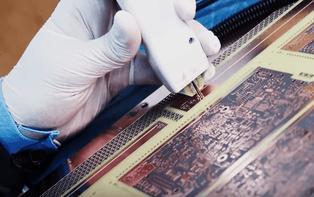
# The cross-section analysis
How do we ensure that you get what you are asking for? We perform a cross-section analysis of the panel and measure the relevant thickness. This ensures that there is a good connection to the inner layers and also that the copper wrap is even throughout the hole. For IPC Class 3 board design, there are different requirements that also include CAF and etch-back.
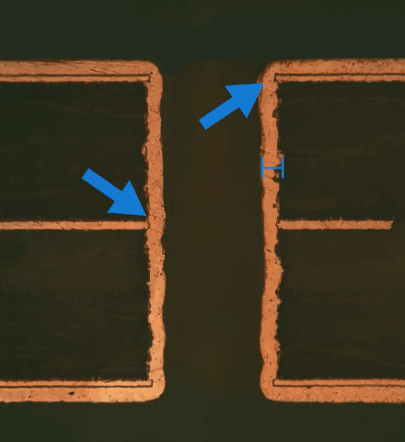
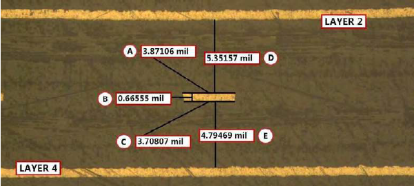
Failure analysis: Upon failure, a cross-section of the impedance coupon is taken to investigate the deviation from the calculated impedance to the recorded impedance. The manufacturer’s cross-section technician measures the dielectric thicknesses depending on the trace location, either the inner layer or the outer layer. Additionally, the trace width is estimated from the bottom as well as from the top of the affected impedance trace, along with the copper thickness or the trace height.
When it is a differential pair, the spacing between the two traces is measured to understand whether or not the projected impedance is in alignment with the recorded impedance. The image shown below depicts the cross-section evaluation details on a single-ended impedance trace.

IPC Class 3 Design Guide
8 Chapters - 23 Pages - 35 Minute ReadWhat's Inside:
- IPC guidelines for manufacturing defects
- IPC standards for assembly processes
- Common differences between the classes
- IPC documents to set the level of acceptance criteria
Download Now
In order to determine the acceptability of the boards, Sierra Circuits uses test coupons to make sure there are no variations in trace width, trace thickness, and so on. We manufacture the test coupons on the same panel and under the same specifications as the actual boards, which are too difficult to test because controlled impedance traces are hard to access and often do not have any trace work or pads.
# The TDR testing
Now that we know we have the key measurements manufactured properly, we use a Time Domain Reflectometer (TDR) machine to test that the ohms are accurate. The TDR machine checks whether the model that we created, in the beginning, is accurate or not. You will see the TDR report in the documentation that goes with the order. Get more insight on our blog on how TDR impedance measurements work.
# Get help with your stackup
The stackup design is very crucial for the manufacturing of a controlled impedance PCB. The designer needs to create a stackup for the board and then calculate the trace values for differential pairs and single-ended nets. To calculate the values, the designer needs to know the following information:
- Number of board layers
- Layers on which to route controlled impedance traces
- Layers to use as reference layers
- PCB materials used and copper thicknesses on various layers
- Dielectric constant and dielectric height (when modeling yourself, it is a good idea to use a 4 mil dielectric height for inner layers and 3 mil for outer layers)
If your board is fairly complex with lots of impedance on multiple layers, then it is customary for us to build an initial stackup model for you. If your requirements are not so strenuous, you can also use our free online stackup and controlled impedance tool. It is a free 2-D field solver and will get you where you need to be for trace and space requirements and overall board thickness limitations.

Mistakes to avoid in a stack-up while manufacturing controlled impedance PCBs
# Type of prepregs
It is recommended not to use more than three different types of prepregs in a stackup. Furthermore, the dielectric thickness of each prepreg layer should be less than 10 mils. Otherwise, it increases the chance of a greater variation in the final thickness. You should avoid using prepregs with very low resin and high glass content: very low resin content may lead to resin starvation during lamination.
Examples of very low resin and high glass content prepregs are those that use 7628 and 2116 content glass styles. 2113 glass style is a borderline case. If possible, avoid it in a prepreg layer unless there are no adjoining copper layers.
# Impedance trace/space
The spacing between two traces in a differential pair should not be more than twice the width of the traces. For example, a 4-mil differential trace should not have more than an 8-mil space. The trace width should also not exceed twice the dielectric thickness between the target signal layer and the nearest reference layer.
# Average effective dielectric constant calculation
When there are several types of dielectric materials (having different dielectric constants) between the signal layer and the reference plane, it becomes necessary to calculate the effective dielectric constant of the composite dielectric material. A simple way is to calculate the weighted average of the dielectric constant is stated below:
How to document controlled impedance requirements in the PCB design?
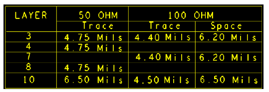
A layout designer must include the impedance information in the fabrication drawing notes and tables. The information should include the impedance value, the trace width, the spacing for differential pairs, and the layer on which the controlled impedance traces are routed. Preferably, an impedance table should be provided in the fabrication drawing. Here is an example of a table:
The figure below provides an example of how to specify controlled impedance on a fabrication drawing:
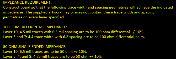
The PCB manufacturer will review these notes and create a stackup to get the desired trace width and spacing specified in the notes. They can make minor adjustments in the trace width and spacing to achieve the desired impedance.
Manufacturers can now model controlled impedance while manufacturing PCBs more accurately through new tools and detailed data about PCB materials. Getting a good PCB with accurate controlled impedances needs a proper selection of PCB material and control of dimensions such as trace thickness, trace width, and dielectric thickness. Sierra Circuits provides stackup design tools and services. Before starting the layout design, it is necessary to have a stackup design and to set up the layout tool settings, as stated in the stackup. This includes setting the trace widths of single-ended controlled impedance traces and differential pair controlled impedance traces. Also, setting up 2W and 3W rules between unrelated traces to reduce crosstalk.

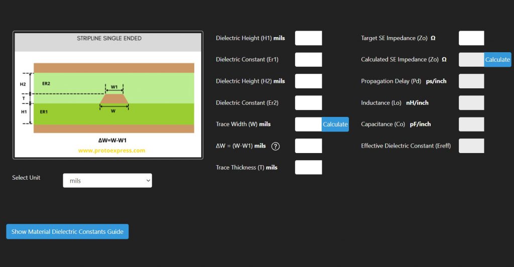
Try Sierra Circuits’ new Impedance Calculator
We have upgraded our Impedance Calculator, a free 3D field solder, which now uses the 2D numerical solution of Maxwell’s equations for PCB transmission lines. It renders accurate results suitable for use in circuit board manufacturing and engineering analysis. In addition to characteristic impedance of a transmission line, the tool also calculates line parameters such as capacitance, inductance, propagation delay per unit length, effective dielectric constant of the structure, and in the case of differential pairs, coupling coefficient, and even and odd mode characteristic parameters.