Hot air solder leveling (HASL) is a widely used PCB surface finish. It is inexpensive and easily available. It also offers a high solderability finish, making it a dominant player in the market for several years. Due to the RoHS directive, there is a major transition from HASL to lead-free HASL.
How is HASL surface finish applied on PCBs?
HASL finish is applied in three steps: cleaning, fluxing, and spraying molten solder to get the required wetting. Afterward, the excess solder is removed with the help of hot air knives. Air knives are devices that are set above the melting temperature of the solder. The circuit board is run through a washer to remove flux residues after the solidification of the solder.
Most HASL lines are vertically designed to fully immerse the PCB in a bath of solder and thus provide a high-quality finish. Do note that horizontal lines can also be used. Here the board is flooded with solder through nozzles or rollers attached to the top and bottom of the panel. The horizontal process offers a better uniform thickness than the vertical procedure due to the zero impact of gravity on the solder distribution.
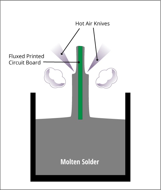
With its excellent wettability, HASL’s solderability is superior to other finishes. Moreover, it can preserve solderability for a long period without requiring additional protection. The finish quality is determined by air pressure, the rate at which boards enter and move away from the solder, and the angle of air knives.
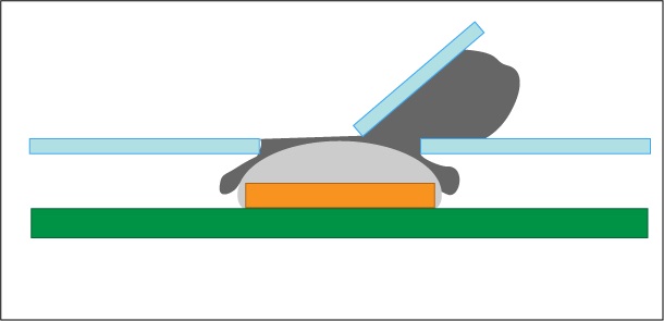
It is an effective method for soldering components, but the surface may not be suitable for fine-pitch components because of its thickness. HASL deposit is composed of a tin and lead eutectic mixture. It is a good choice if you’re using through-hole or larger SMT components. However, this is not ideal if the board contains SMT components smaller than 0805 or SOIC. This surface finish exposes the PCB to temperatures up to 265°C and can recognize potential delamination issues before attaching expensive components.

Design for Manufacturing Handbook
11 Chapters - 96 Pages - 90 Minute ReadWhat's Inside:
- Annular rings: avoid drill breakouts
- Vias: optimize your design
- Trace width and space: follow the best practices
- Solder mask and silkscreen: get the must-knows
Download Now
Characteristics of hot air solder leveling
- Consists of a longer processing window. It can be readily used during manufacturing schedules that do not require large amounts of boards to be produced quickly.
- Offers a better aesthetic value.
- Maintains uniform coating thickness. This thickness depends upon the volume of solder remaining on pads after passing through a hot air knife and surface tension forces.
- Subsequent soldering processes will result in non-wetting and/or dewetting when the solder coating does not fully cover the intermetallic layer. Reasons for dewetting include:
- Insufficient preparation of copper surfaces to achieve complete wetting with the fluxes used, the solder temperatures, and contact time exposed during HASL.
- Hot air knives were positioned such that not enough solder was left on the pads for surface tension forces to adequately cover the pad.
Advantages and disadvantages of hot air solder leveling
The advantages are as follows:
- HASL is economical and widely available.
- It has excellent solderability and good shelf life.
- It is reworkable.
The disadvantages include:
- HASL is harmful to the environment and violates RoHS compliance.
- It is not suitable for fine-pitch components and plated through-holes.
- It can cause poor wetting.
Also, see types of circuit board surface finishes.
Transition from tin-lead HASL to lead-free HASL
Due to strict RoHS regulations, most companies are preferring lead-free HASL instead of tin-lead HASL. Lead-free HASL uses lead-free alloys and offers a smooth, even, and high-quality surface finish. This finish is highly solderable and environment-friendly. Coating thickness is more uniform and thus eliminates coplanarity issues caused by the HASL process (on BGA, CSP pads, etc.). It is superior to HASL as it avoids the most common problems such as:
- Stencil gasketing during solder paste printing
- Coplanarity concerns due to pad to pad variation in the coating thickness
- Board damage because of extra thermal excursions
Lead-free HASL maintains solderability through many lead-free reflow profiles. Nowadays, there is a growing need for this finish and a minimum requirement of tin-lead finish.


