Array panelization is a manufacturing technique that reduces cost and simplifies the PCB assembly procedure. This technique involves the production of multiple copies of a board (with the same or different designs) by placing them in an array on a standard panel. Later, depanelization is performed using either breakaway tabs or V-scoring. Generally, breakaway tabs produce mouse bites after detaching the board from the manufacturing panel.
What is a PCB array?
Many circuits are very small compared to the panel on which they are printed. To avoid wastage, these small circuits are printed multiple times on the same panel. This is called an array of circuits. Accordingly, a circuit board array is a combination of smaller-sized individual boards connected together to form a larger array of circuits.
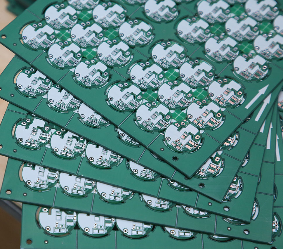
All the modern assembly machinery comes with sliding rails that can accommodate these PCB panels. Moving smaller individual boards along these rails one by one would increase the time required for component placement. Hence board arrays on large panels are used.

PCB Design for Assembly Handbook
6 Chapters - 50 Pages - 70 Minute ReadWhat's Inside:
- Recommended layout for components
- Common PCB assembly defects
- Factors that impact the cost of the PCB assembly, including:
- Component packages
- Board assembly volumes
Download Now
Placement of boards in an array
The panel array is designed with specific CAD software. The Gerbers of the circuit are imported into the software and replicated multiple times. The placement of these Gerbers is optimized to get the maximum number of PCBs.
Boards should be rotated and flipped in order to accommodate the maximum possible number in the array. After placing the boards, a Gerber file is generated for the whole panel.
The individual PCBs arranged in a panel should ideally be oriented (rotated) in the same direction. If they are rotated 180 degrees off of each other, i.e., if one column of boards is flipped 180 degrees with respect to its neighboring column, then the automated machines performing component placement will undergo extra labor. The same is the case with AOI inspection machines.
But sometimes to accommodate more circuit boards in a single panel, they might have to be rotated (inclined). In such cases, it is financially beneficial.
How are circuits separated in a PCB array?
Two common techniques of separation are V-scoring and tab routing.
V-scoring/routing
In this method, the individual circuit boards are separated from each other using V-shaped grooves. An angled blade removes one-third of the board material at the top and bottom.
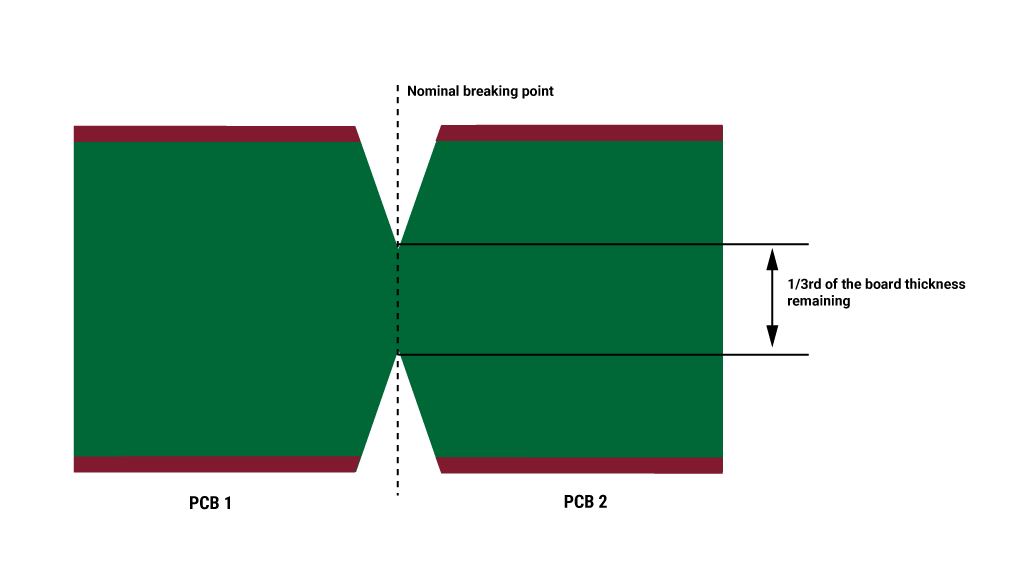
The main limitation of this method is that it cannot be used when there are components hanging over the edges. V-scoring can also weaken the board array which is not ideal when they have to be wave-soldered. To resolve this issue, we perform jump scoring in PCB panels.
Tab routing panelization
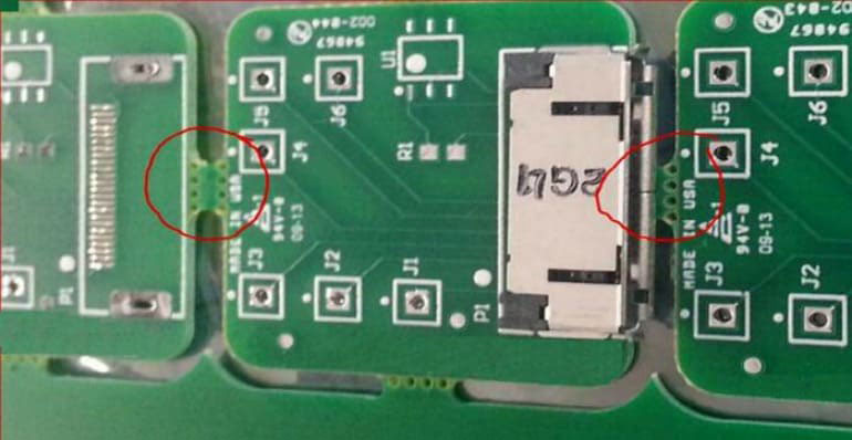
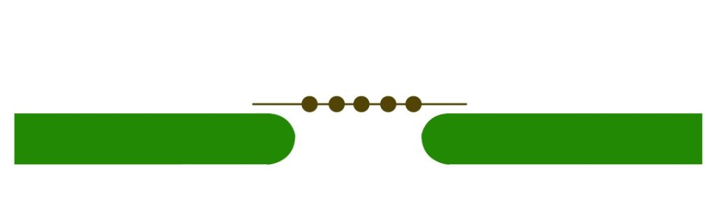
When the V-scoring technique cannot be used, perforated tabs are employed in between the individual boards. The holes provided in these tabs are called mouse bites. The traces and the surface-mount components are placed at least 3 mm away from these holes. This is to avoid the damage caused to them during board separation after assembly.
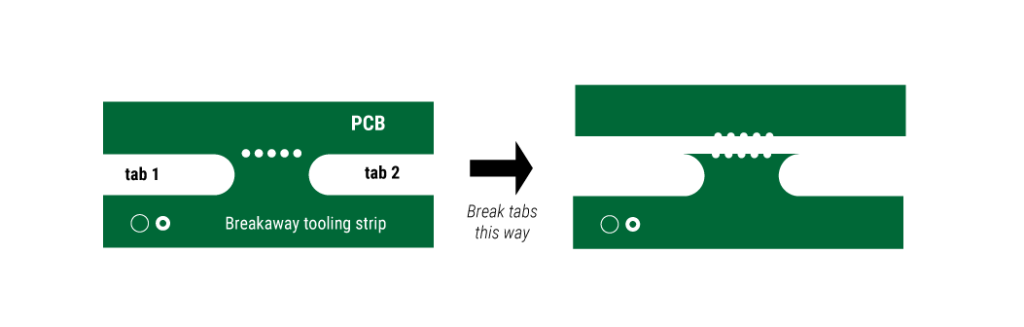
A five-hole perforation or a three-hole perforation pattern is used as the standard for these tabs. This is chosen based on the available clearance. In panels where the clearance is limited, three-hole tabs are employed. These tabs should not be placed under overhanging parts.
What are mouse bites in circuit boards?
Mouse bites are microscopic perforated holes that are used during the board array panelization. After completion of the depanelization process, the breakaway tabs need to be removed to free the board from the manufacturing panel. For each broken tab, the remnant material scraps will be popped up like mouse bites. They are later smoothened out.
Dimension and spacing of mouse bites
The hole diameters and the separation distances for mouse bites in PCB do not possess any specific rules. For smaller holes, it will take less effort to smoothen the scraps out. Holes with a small diameter require more drilling and leave more residue material. However, if you employ a larger hole, it will be tedious to smooth out the larger mouse bites. The most commonly implemented hole diameter is 0.5 mm (0.020 inches).
Positioning the holes within the breakout tab is crucial. The aim is to locate them closer to the board outline so that it will be easier to extract the leftover material. The typical spacing between two holes is 0.76 mm (0.030 inches). However, the fabricator may change this value as per the requirement.
Constraints to keep in mind while placing breakaway tabs
- Incorporate sufficient tabs to secure the board tightly with the manufacturing panel.
- Avert using unnecessary tabs, which can increase the stress of the board and also waste your time and effort.
- Do not locate them adjacent to sensitive components to avoid mechanical and electrical damage.
- Place breakaway tabs with a slight inset (as shown in the image below) to reduce the labor to clean up.
Comparison between breakaway tab routing and v-grooving
| Tab routing | V-scoring |
|---|---|
| Components can be allowed to place near the board edges by varying the positions of the tabs. | There must be an adequate gap between the components and the board edges. |
| Implemented for odd-shaped PCBs. | Implemented for rectangular or square-shaped PCBs. |
| Smooth edges can be achieved by sanding the residue material. | Leaves rough edges. |
| Requires more time. | Consumes less time. |
| Expensive due to greater amount of residues. | Less expensive because of reduced residues. |
Depanelization of circuit board arrays
Depanelization is the process of splitting the individual boards from the array after assembly. The following are the methods of depanelization:
- Breaking by hands: This option is only suitable for arrays that are easily breakable.
- Pizza cutter machine: This machine is used only in the case of V-scored/routed arrays. They are hard to separate using hands. This method is cost-effective and requires low maintenance.
- Punching: In this process, a two-part fixture is used. This fixture punches out the individual boards from the array. This technique can be used for high volumes but the maintenance of this fixture is high.
- Saw: A saw can be used for cutting both V-grooved and non-V-grooved arrays. This can perform cutting at a good speed.
- Laser: Lasers can also be used for carving out individual boards from the arrays.
Array panelization saves time and labor during high-volume fabrication. Therefore, it is important to take the necessary steps during the paneling and depanelizing of arrays.


