What is a plated-through slot?
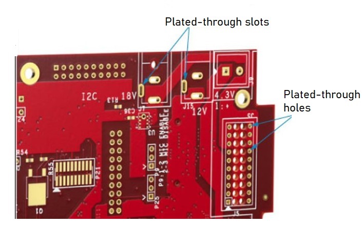
A plated-through slot (PTS) is required to place through-hole components with rectangular leads on a PCB. These slots serve the same purpose as plated-through holes. They physically connect the components to the board and also provide an electrical connection.
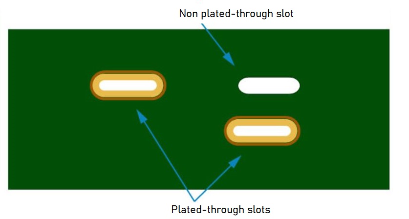
Plated-through holes accommodate the leads of the through-hole components. The leads of these components are thin and can be mounted easily on a circular hole. But when it comes to components with rectangular leads, they cannot be accommodated inside a standard hole. Even if they do, there will be unwanted spaces. Hence a better option is to create slots that are more suitable for rectangular leads.

Design for Manufacturing Handbook
11 Chapters - 96 Pages - 90 Minute ReadWhat's Inside:
- Annular rings: avoid drill breakouts
- Vias: optimize your design
- Trace width and space: follow the best practices
- Solder mask and silkscreen: get the must-knows
Download Now
Benefits of plated-through slots
Using plated-through slots reduces unwanted spaces between the component leads and the position that accommodates them. Hence, when slots are used for big rectangular leads, there will not be any unnecessary gaps left after the component placement. This reduces the chances of solder joint voiding. Apart from this, accurate slots for leads will also free up more space on the circuit board surface.
Also, see castellated holes or plated half-holes for reliable board-to-board edge connections.
How do I create PTS?
To fabricate a plated-through slot, the manufacturer needs to have a clear idea about the requirements. Care should be taken in the design stage to designate these slots accurately. The length and width of each slot should be mentioned in the fab drawing.
To designate a slot in your EDA tool, you need to add an oval-shaped hole. The plated-through slots can also be defined in the Gerber mechanical layer. If there are no mechanical layers in your design file, then add one and define the slots. Also, use a README file to define your slot requirements.
Fabricating plated-through slots
The minimum width of a plated-through slot is 0.5mm. The first step is milling the slots in the required dimensions. This process removes the unwanted copper from the board surface, so that traces, pads, and other required structures are formed as per the layout. Next, the slots are drilled using an appropriate drilling method as per the design requirement. Drilling is followed by cleaning the slots to remove any residues. Later, these slots are copper plated. The process of plating is the same as that of plating through holes, using an electroless copper deposition method. In the final step, slots are given a surface finish.
When it comes to accommodating through-hole components with rectangular and unconventional leads, then opting for through-holes will create extra unwanted space inside the hole. To eliminate this, it is always ideal to create through-slots that are precisely in the same shape as the leads and hence, will provide a better fit.


