Tools for Designers:
PCB Stackup Designer
Start Building Your Stack-UpSierra Circuits’ PCB Stackup Designer helps you create advanced, manufacturable stack-ups in real-time, perfect for high-speed, flex, and complex BGA designs.
With this easy-to-use web app, you can export IPC-2581 files and generate outputs compatible with Altium Designer® and Cadence Allegro®.
Key features of the PCB Stackup Designer
- Comprehensive layer stack library: You can choose from pre-designed stack-up templates for standard, high-power, high-frequency, and HDI applications.
- Integrated with PCB design tools: The stack-up tool has built-in calculators that help you optimize your layer stack to maintain signal integrity. They include the following calculators:
- Signal loss
- S-parameter
- Crosstalk
- Via current capacity and temperature rise
- Trace width, current capacity, and temperature rise
- PCB conductor spacing and voltage
- BGA-optimized stack-ups: Customize stack-ups for complex BGA layouts using pitch, pin count, and pattern details.
- Compatible with various EDA tools: Save your stack-up to your project or export it in IPC-2581 format for EDA tools like Altium Designer and Cadence Allegro.
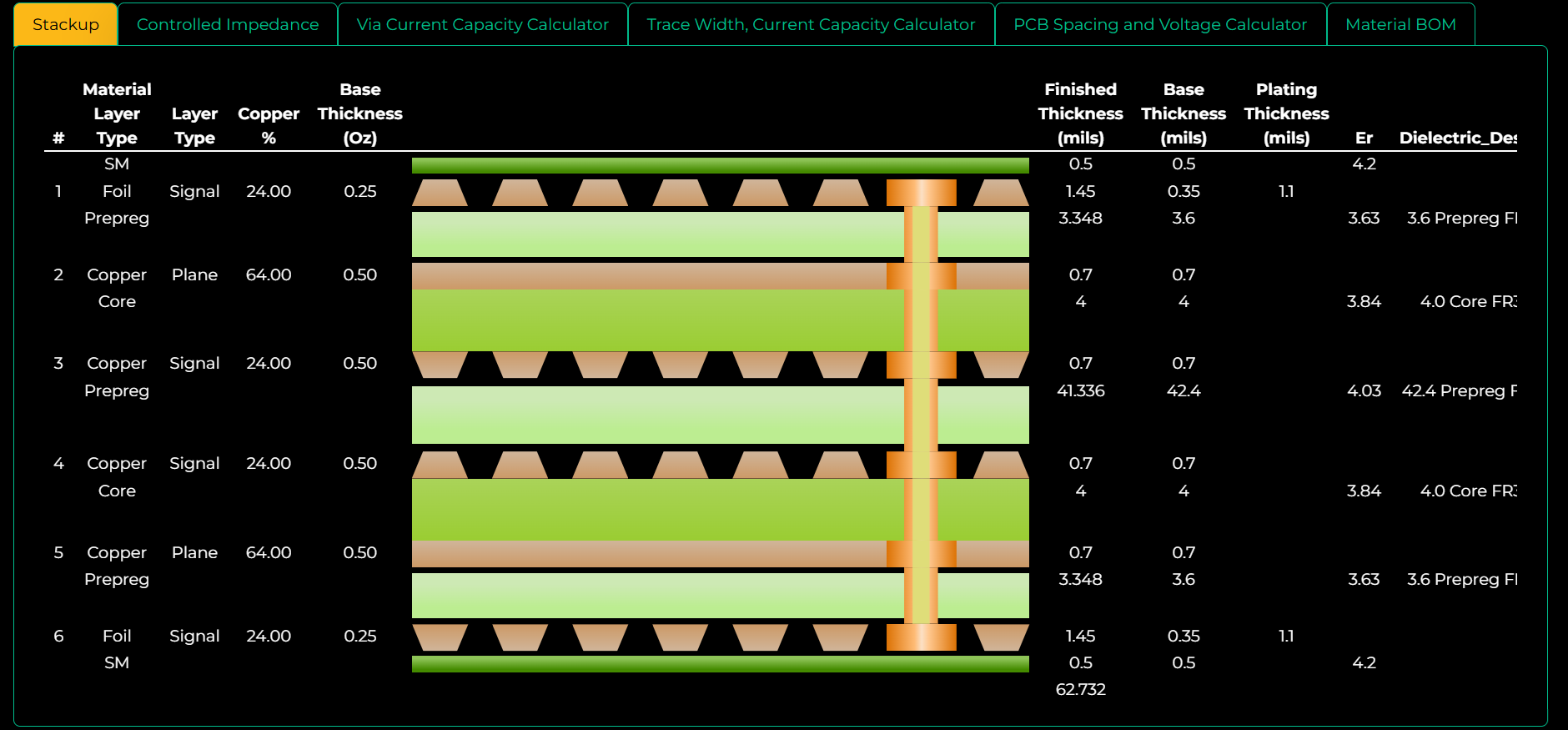
- Real-time visualization: View layer-by-layer construction details, including material type, copper thickness, and dielectric properties.
How to use the PCB Stackup Designer
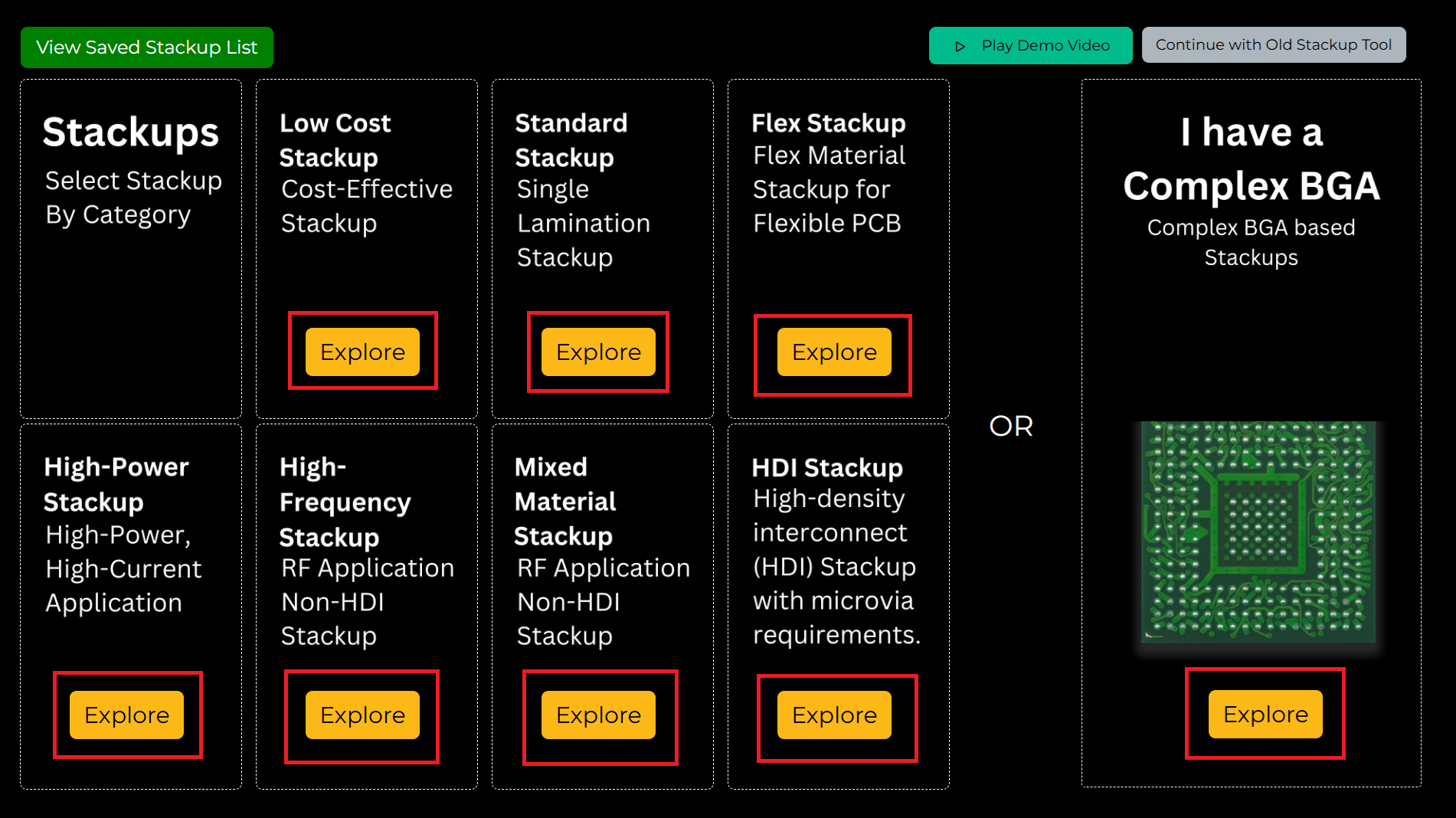
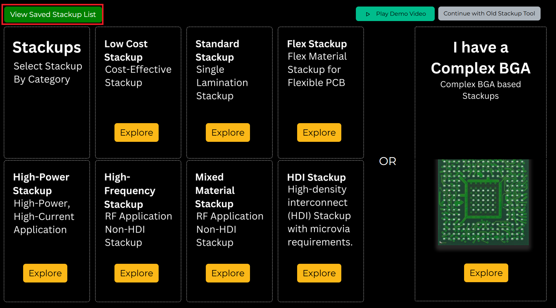
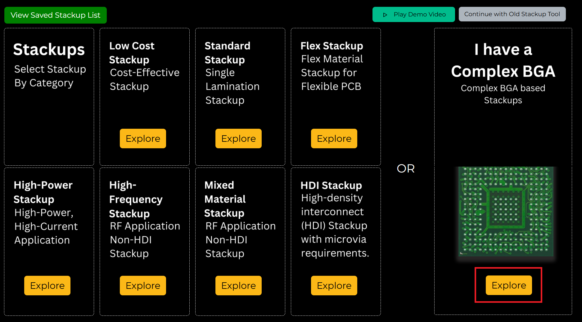
Choose the relevant stack-up category and select the required stack-up from the following options:
- Category 1
- Low cost
- Standard
- Flex
- High-power
- High-frequency
- Mixed material
- HDI
- Category 2
- Complex BGA- If your design includes complex BGAs, select this option.
Click on the respective Explore button to select your stack-up.
Steps to generate stack-ups for category 1
This section shows the steps to create build-ups for low-cost, standard, high-power, high-frequency, and HDI PCBs. If your design includes BGAs, skip to the next section: Steps to generate a BGA-based stack-up (Category 2).
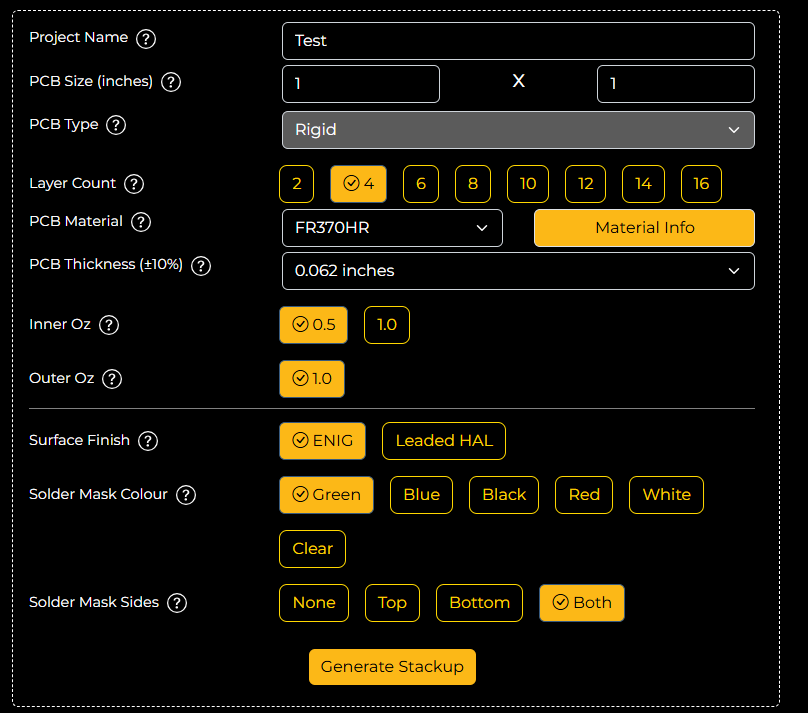
Step 1: Provide the following project details:
- Project name
- PCB size (length and breadth)
- Layer count
- PCB material
- PCB thickness
- Inner copper weight (Oz)
- Outer copper weight (Oz)
- Surface finish
- Solder mask colour
- Solder mask sides
Note: Surface finish, solder mask colour, and solder mask sides fields do not apply to flex boards.
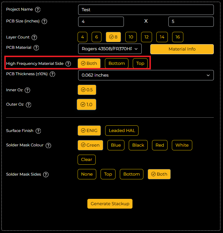
If you’re working on a mixed material design, select the high-frequency material side (Both/Bottom/Top).
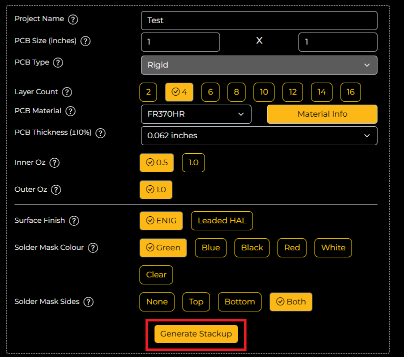
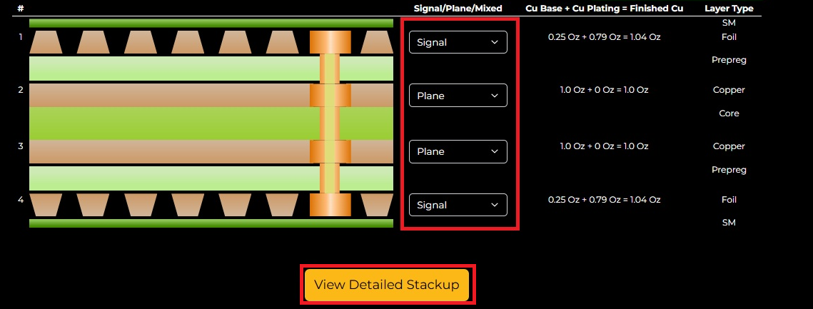
Step 2: Click Generate Stackup. The tool will display the recommended build-ups based on your inputs.
You can modify each layer using the relevant dropdowns.
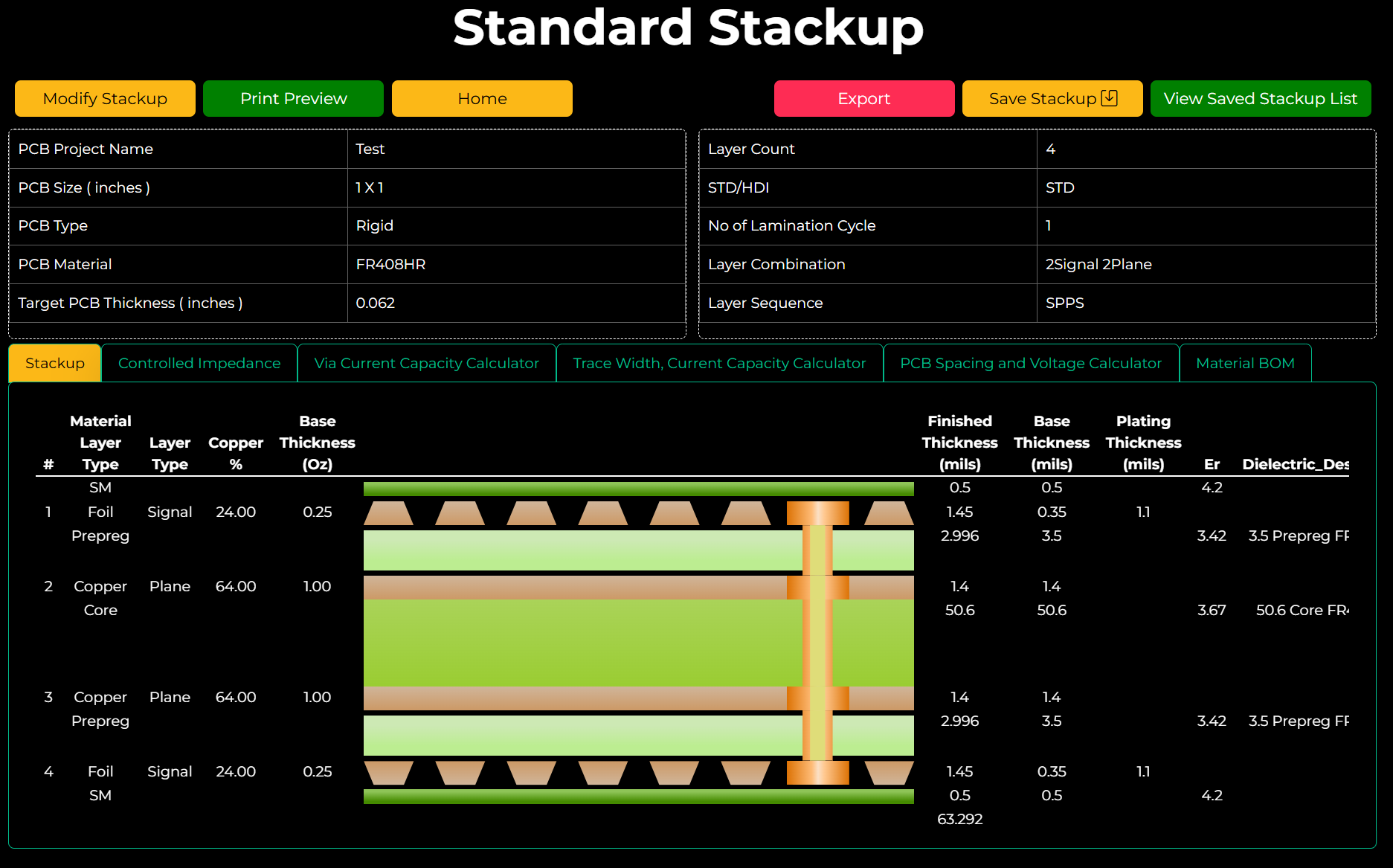
Step 3: Click View Detailed Stackup to see a comprehensive breakdown of your build-up.
Here, you can view the layer type, copper percentage, base (start copper) thickness (Oz), finished thickness (mils), base (finished copper) thickness (mils), plating thickness (mils), dielectric constant (Er), dielectric description, stackup construction, and dissipation factor (@10GHz).
If you wish to edit your build-up, hit Modify Stackup and select Yes. This loads the input page, as shown in step 1. Make the necessary changes and follow the same steps (steps 2 and 3).
Step 4: Define your controlled impedance, via, trace, and spacing details.
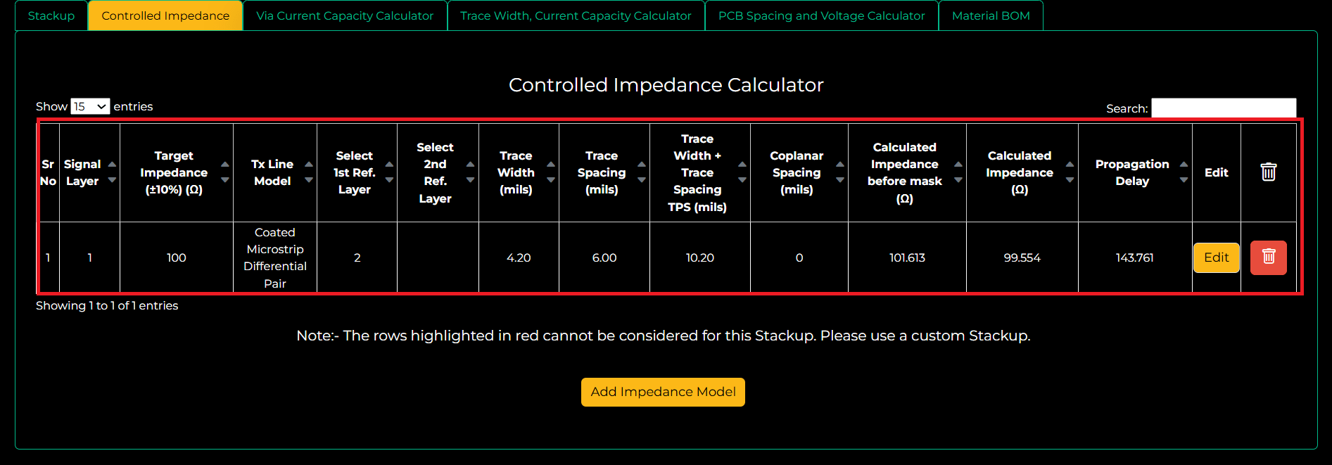
To set your impedance requirements, navigate to the Controlled Impedance tab and hit Add Impedance Model.
Next, select the model type from the dropdown.
The options include:
- Single Ended: Specify impedance layer number, target impedance (±10%), and reference layers (1st ref., 2nd ref., or both).
- Differential Pair: Specify impedance layer number, target impedance (±10%), trace separation (S), and reference layers.
- Coplanar Single Ended: Specify impedance layer no., target impedance (±10%), coplanar spacing (CS), coplanar width (CW), and reference layers.
- Coplanar Differential Pair: Specify impedance layer no., target impedance (±10%), trace separation (S), coplanar spacing (CS), coplanar width (CW), and reference layers.
After selecting the impedance models, click Add. The calculated impedance values will be displayed as shown below. Here, a coated microstrip differential pair impedance model has been added to the table.
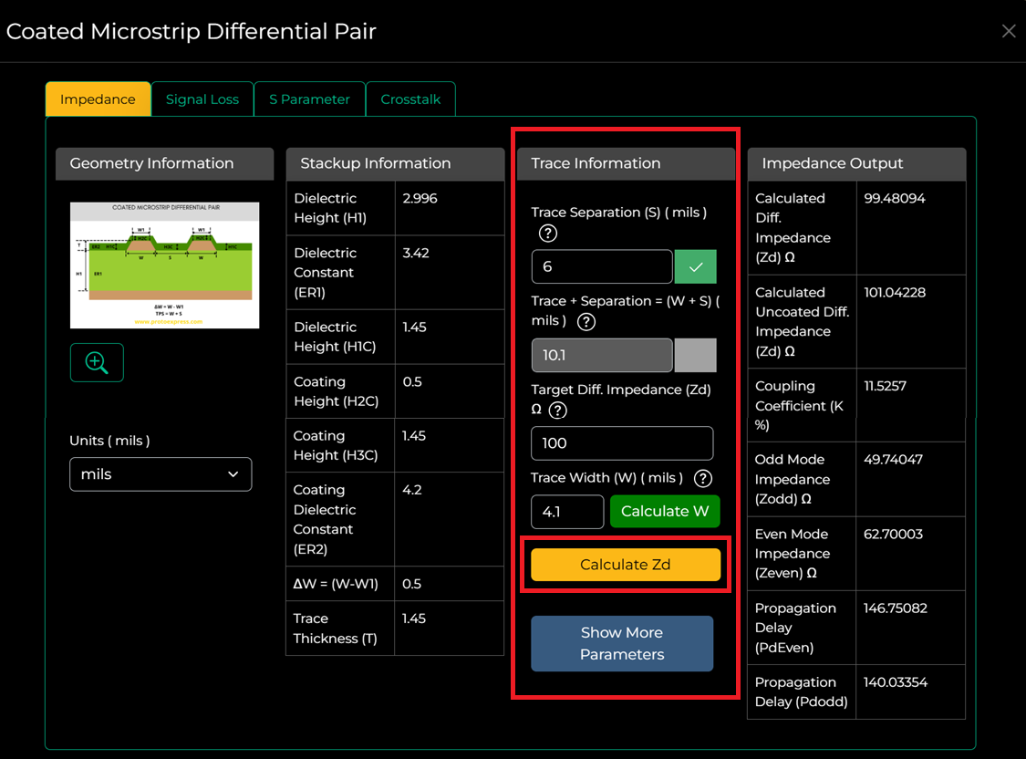
If you’d like to change the impedance model, click on Edit. A pop-up displays the impedance calculator along with the signal loss, S-parameter, and crosstalk calculators.
Here, you can change any of the trace parameters and recalculate the width or impedance by clicking Calculate W or Calculate Zd, respectively.
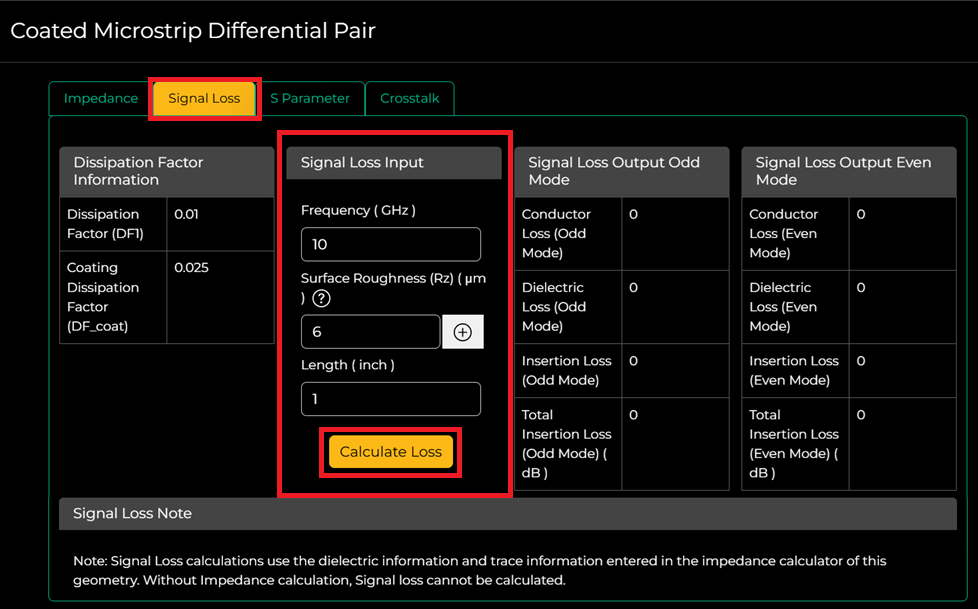
To calculate the signal loss in odd and even modes, select the Signal Loss tab. Enter frequency, surface roughness, and length, and click Calculate Loss.
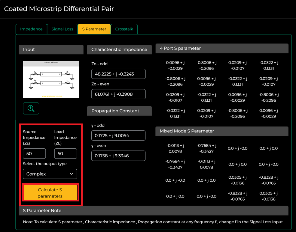
To calculate the S-parameter matrices, characteristic impedance, and propagation constant at any frequency, select the S Parameter tab. Enter the source and load impedances and select the output type (complex or polar) using the drop-down. Click on Calculate S parameters.
Note: The S-parameter matrices are calculated based on the frequency input during signal loss calculation.
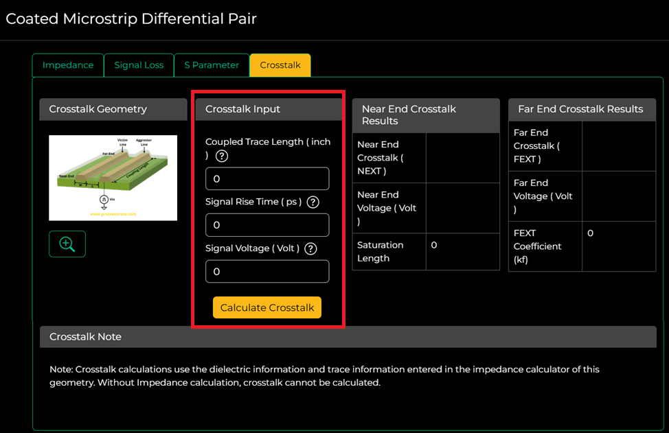
To calculate near-end and far-end crosstalk, select the Crosstalk tab. Enter the coupled trace length, signal rise time, and signal voltage, and click on Calculate Crosstalk.
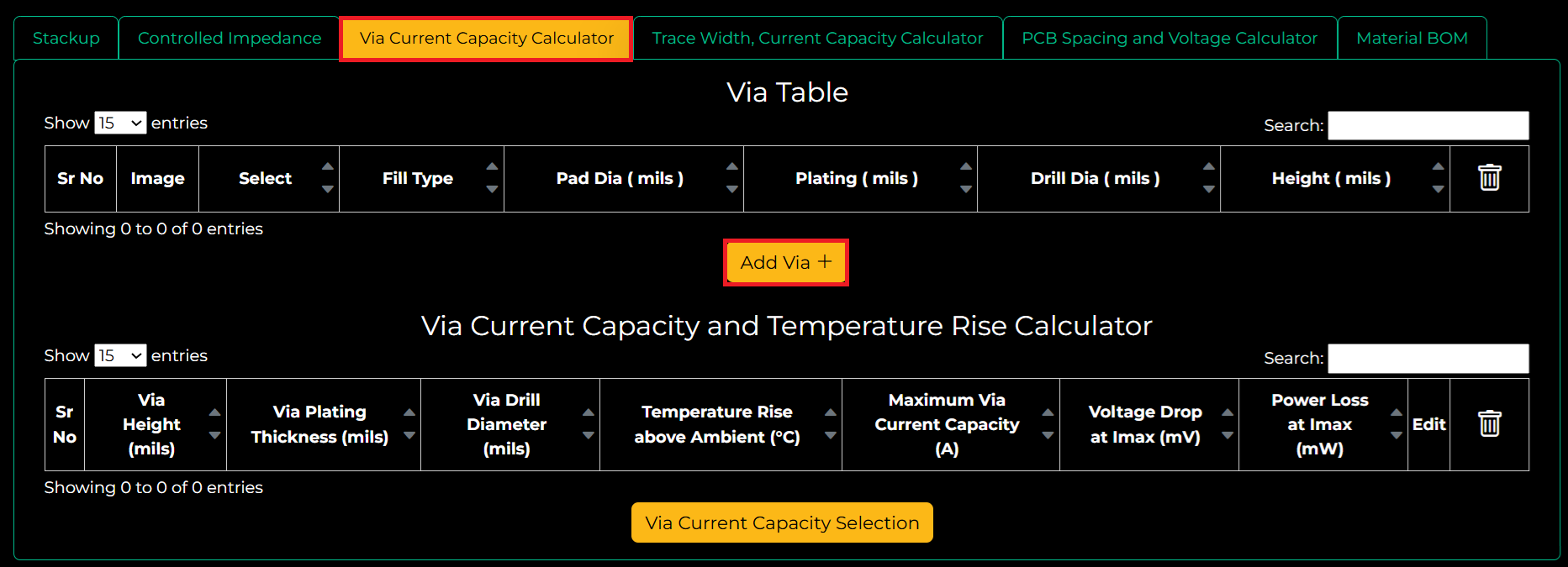
To add plated holes to your stack-up, go to the Via Current Capacity Calculator and hit Add Via +.
Next, select the via type, enter the drill and pad diameters, and click Add.
Note: If you’re unsure about the via pad diameter, click Calculate Via Pad to determine it based on the via drill diameter.
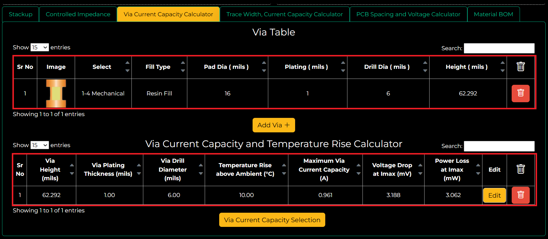
Simultaneously, the tool calculates temperature rise above ambient, maximum via current capacity, voltage drop at Imax, and power loss at Imax for your via. The results will be displayed as shown below.
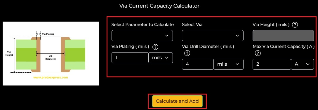
To calculate the via current capacity for a specific drill diameter or vice versa, click on Via Current Capacity Selection.
Next, select the parameter you wish to compute (Via Drill Diameter/Maximum Via Current Capacity) and choose the via from the Select Via dropdown.
Enter the via plating thickness and the known parameter (Via Drill Diameter/Maximum Via Current Capacity), and hit Calculate and Add.
The tool will now display the via parameters as shown below. You can use this data to add plated holes to your stack-up.
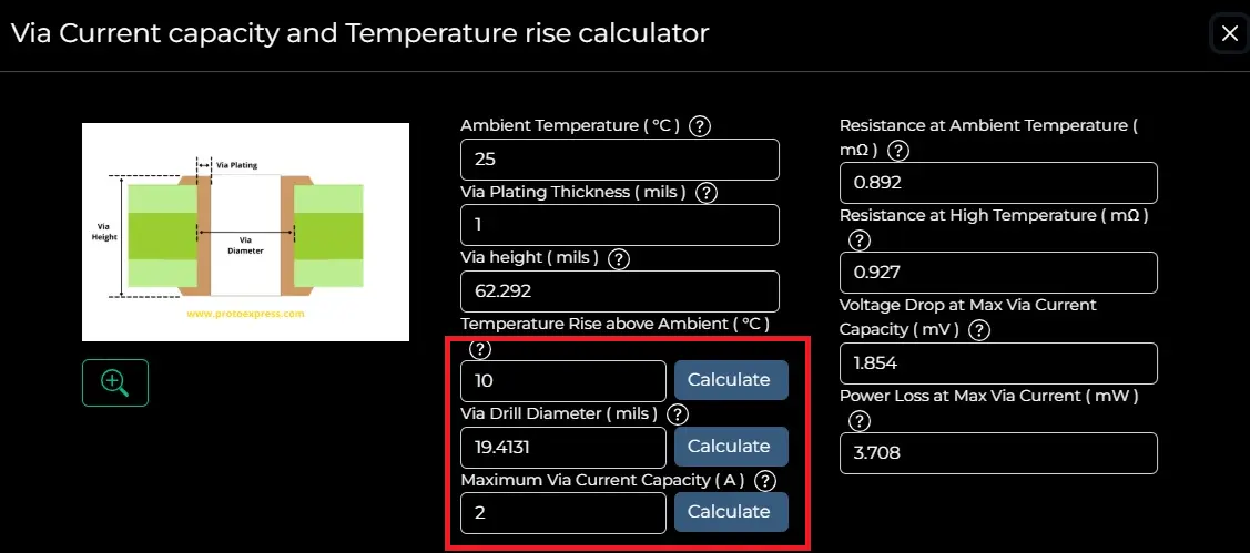
Click on Edit to load the Via Current Capacity and Temperature Rise Calculator. To recalculate, modify the input parameters, and click on the respective Calculate buttons. The updated results will be reflected in the table.
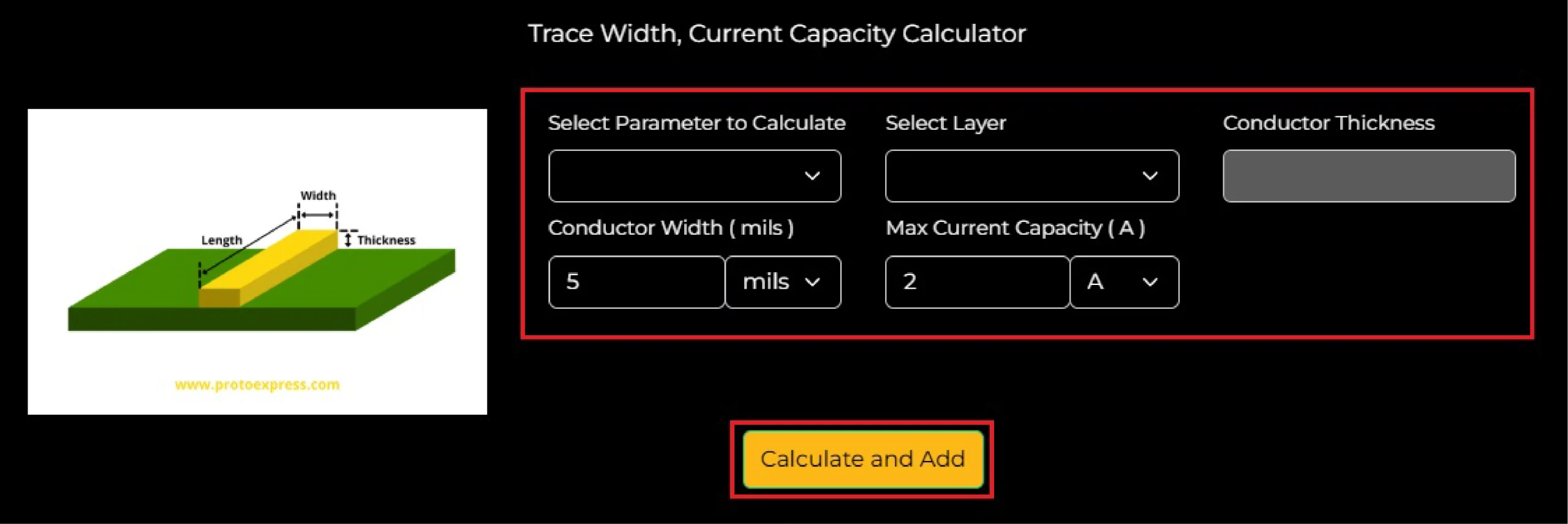
To add traces, go to Trace Width, Current Capacity Calculator, and hit Trace Current Capacity Selection.
Here, you can calculate trace width, current capacity, temperature rise, conductor spacing, and voltage requirements.
Next, select the parameter you wish to compute (Conductor Width/Max Current Capacity) and choose the layer from the Select Layer dropdown.
Enter the known parameter (Conductor Width/Max Current Capacity), and hit Calculate and Add.
The tool will now display the trace parameters as shown below.
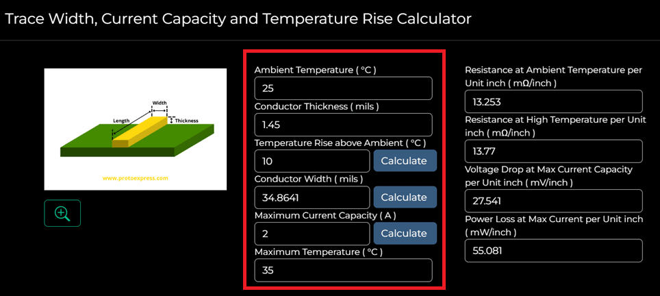
To recalculate, click on Edit to load the Trace Width, Current Capacity and Temperature Rise Calculator.
Next, modify the input parameters and hit Calculate. The updated results will be reflected in the table.
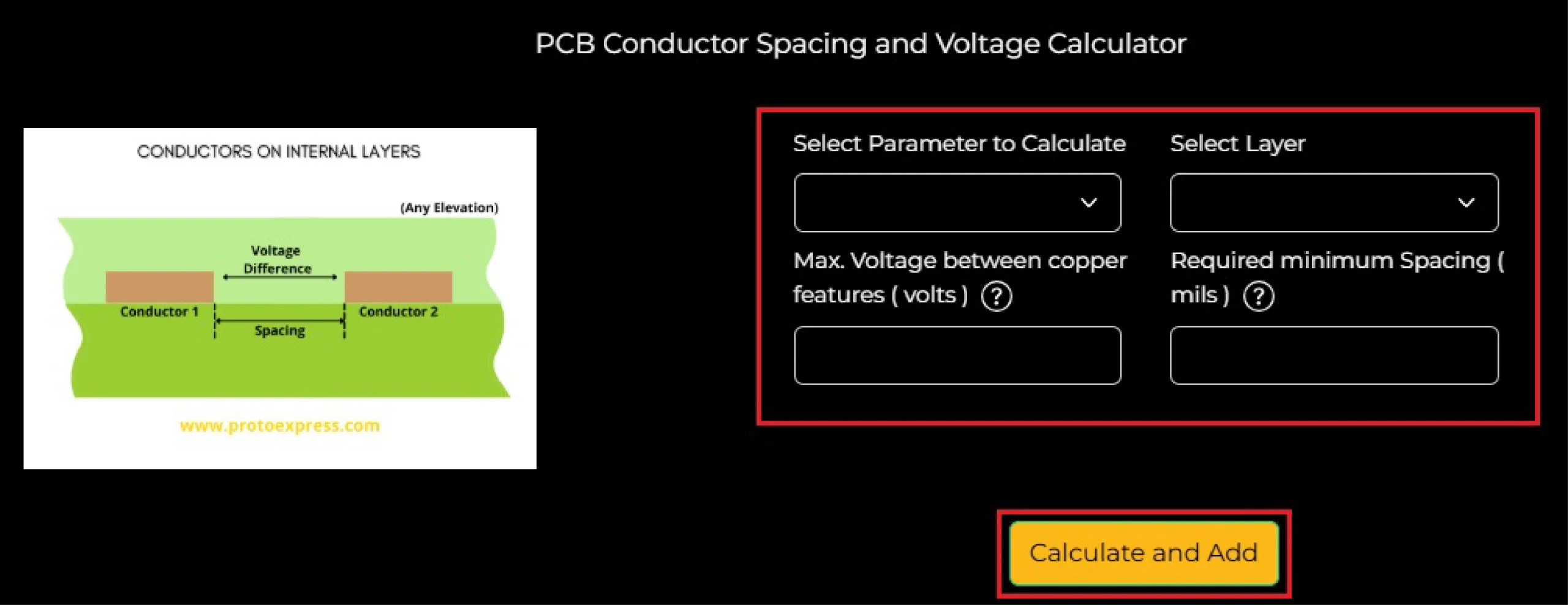
To compute maximum voltage or minimum spacing between copper features, go to PCB Spacing and Voltage Calculator and hit Conductor Spacing Selection.
Next, select the parameter you wish to compute (Max Voltage/Required Minimum Spacing) and choose the layer from the Select Layer dropdown.
Enter the known parameter (Max Voltage/Required Minimum Spacing), and hit Calculate and Add.
The tool will now display the trace parameters as shown below. Click on Edit, and a pop-up window will display the PCB Conductor Spacing and Voltage of External SM Coated Layers Calculator.
To recalculate, modify either of the input parameters (Max. Voltage between copper features/ Required minimum spacing) and hit Calculate. The updated results will be reflected in the table.
Next, go to the Material BOM. This tab displays a table of all the cores, prepregs, and foils used in the stack-up. Here, you can see the construction, resin percentage, thickness, and quantities of the materials used in your build-up.
Step 5: Click Export to download your build-up.
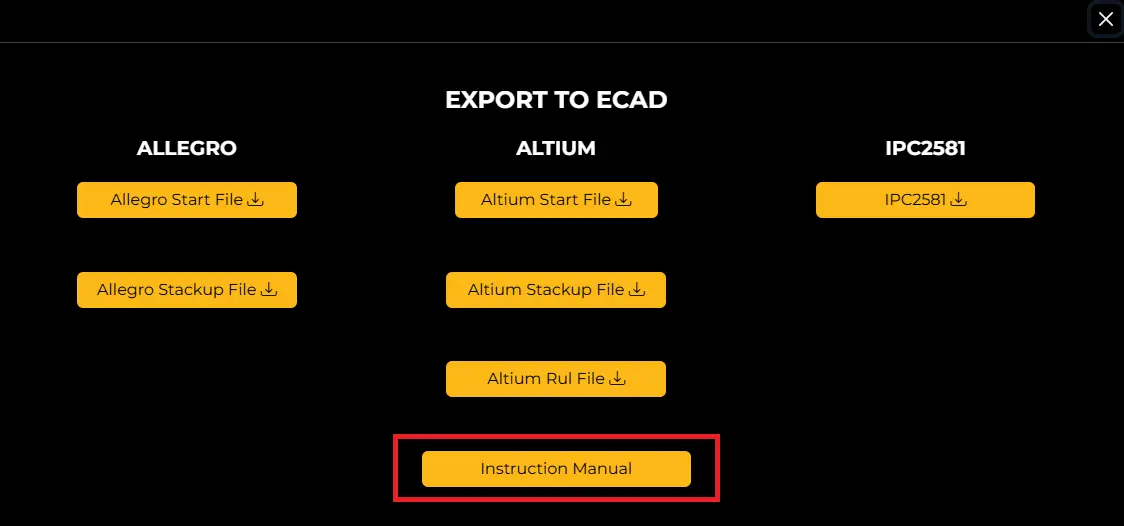
The PCB Stackup designer lets you download files compatible with popular EDA tools like Altium Designer and Cadence Allegro. You can also export your layer stack in IPC-2581 format.
To learn how to import stack-up files into Altium Designer and Cadence Allegro, click on the Instruction Manual to download the guide.
Step 6: Select Save Stackup to save your build-up for future reference.
Steps to generate a BGA-based stack-up for category 2
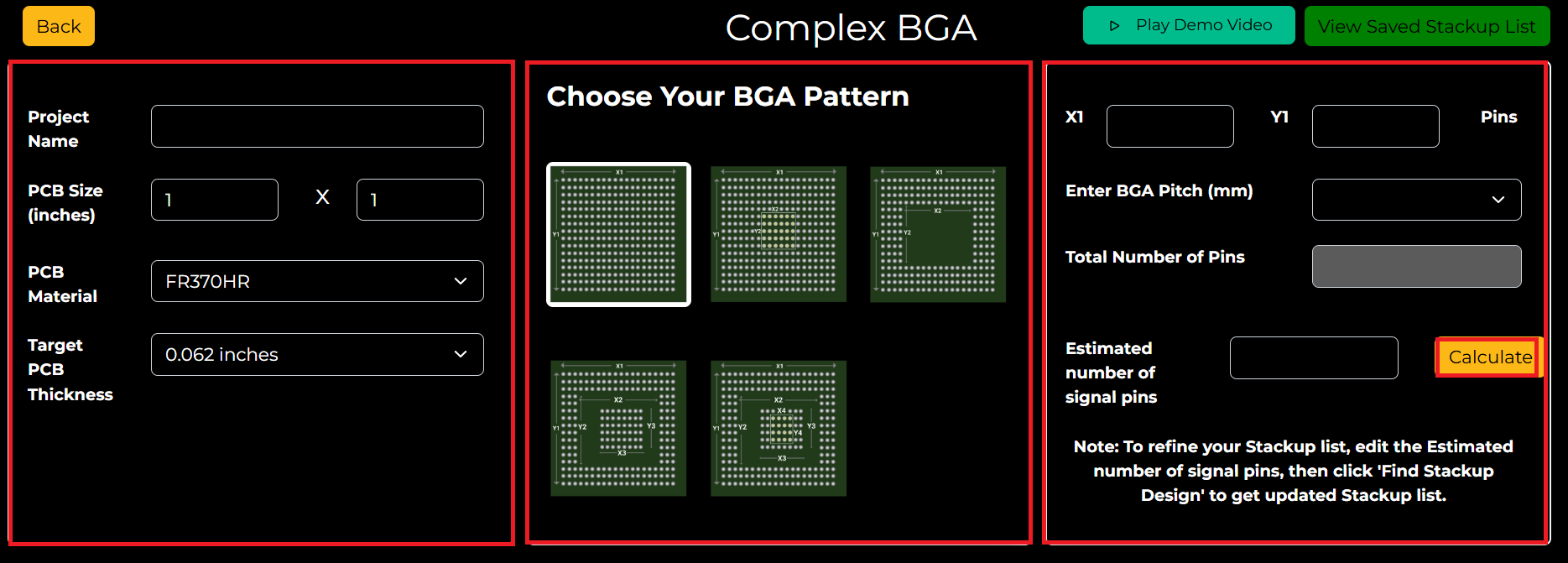
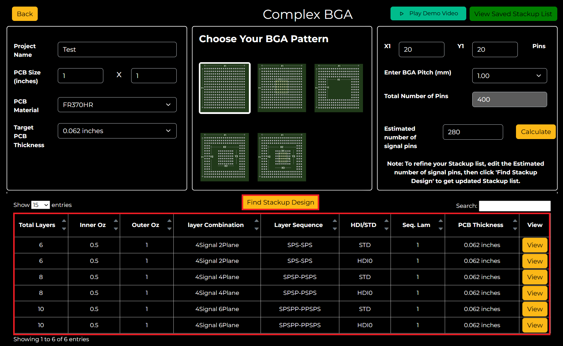
Step 1: To generate a complex BGA-based stackup, click Explore.
- Project name
- PCB size in inches
- PCB material
- PCB thickness
- BGA pattern
- BGA pitch in mm
- X1, X2, X3, X4 (varies based on BGA pattern)
- Y1, Y2, Y3, Y4 (varies based on BGA pattern)
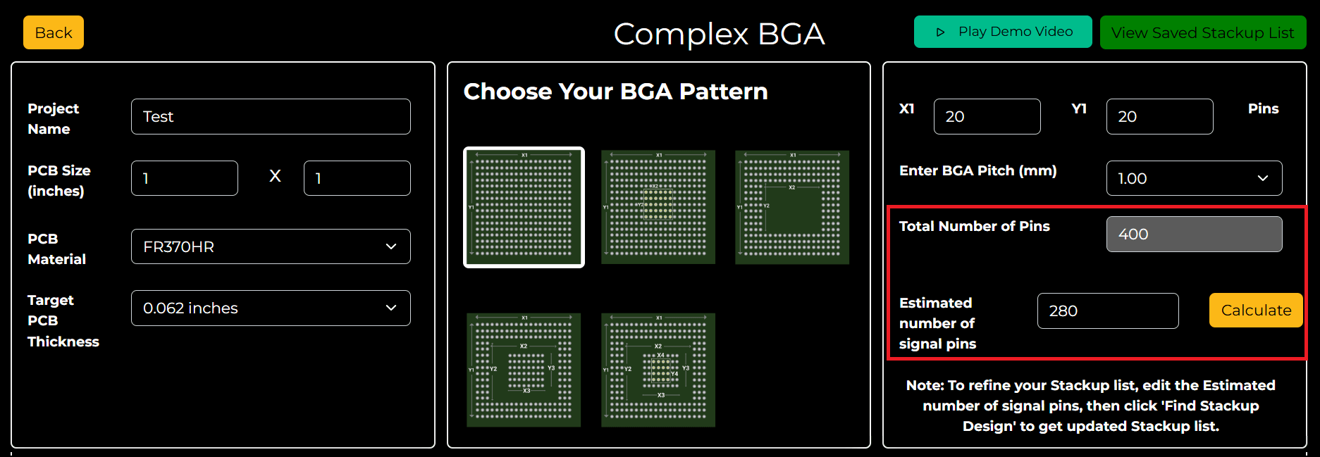
Step 3: Click Calculate to determine the total number of pins and the estimated number of signal pins.
Step 4: Select Find Stackup Design to view a list of available layer stacks.
Click on the respective View button to see the detailed build-up.
Step 5: Define your controlled impedance, via, trace, and spacing details. For this, follow step 4, as shown in the previous section (Category 1). To save and export your stack-up, follow steps 5 and 6.
How to view the saved build-ups
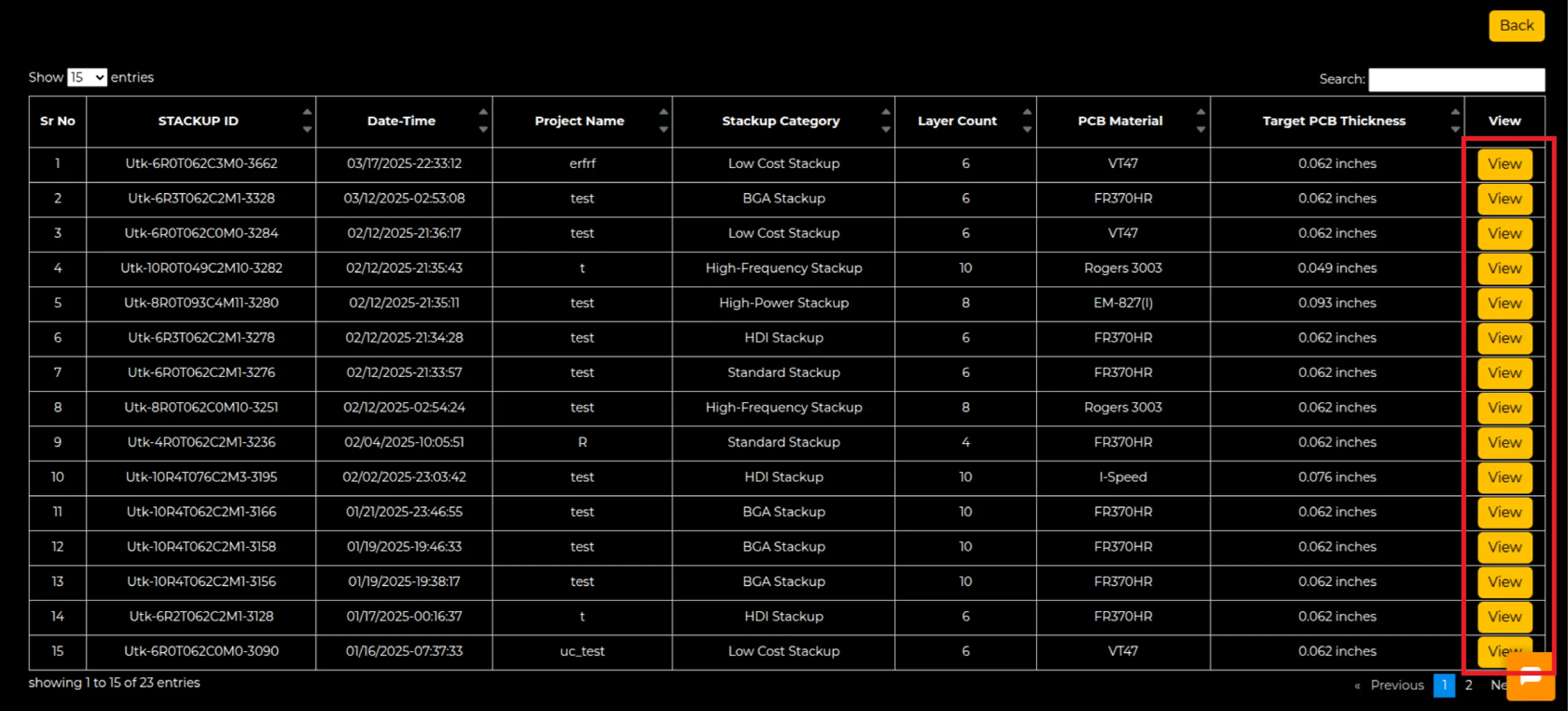
Step 1: Click on the View Saved Stackup List.
This will display a list of all the stack-ups you have saved in a table format, as shown below.
Step 2: Click View to see the detailed stack-up.
The Sierra Circuits’ PCB Stackup Designer simplifies advanced stack-up design with real-time visualization and built-in calculators. It also allows you to easily export your build-up in IPC-2581 format for seamless integration with EDA tools.
Try the PCB Stackup Designer today.
Watch the demo of our Stackup Designer
Sierra Circuits has developed easy-to-use tools for PCB Designers and Electrical Engineers at every stage of circuit board development.
Fabrication, Procurement, & Assembly. PCBs fully assembled in as fast as 5 days.
- Bundled together in an entirely-online process
- Reviewed and tested by Engineers
- DFA & DFM Checks on every order
- Shipped from Silicon Valley in as fast as 5 days
Fabrication. Procurement & Assembly optional. Flexible and transparent for advanced creators.
- Rigid PCBs, built to IPC-6012 Class 2 Specs
- 2 mil (0.002″) trace / space
- DFM Checks on every order
- 24-hour turn-times available
Complex technology, with a dedicated CAM Engineer. Stack-up assistance included.
- Complex PCB requirements
- Mil-Spec & Class 3 with HDI Features
- Blind & Buried Vias
- Flex & Rigid-Flex boards
