


Contents

On-demand webinar
How Good is My Shield? An Introduction to Transfer Impedance and Shielding Effectiveness
by Karen Burnham
The word ‘via’ is originally a Latin word that means road or way. In designing PCBs, vias play a crucial role in interconnection as they are used to route electrical signals between layers.
Vias majorly consist of:
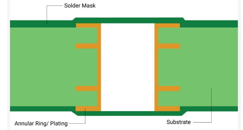
- Conductive barrels that are formed by drilling holes in the panel are made conductive by electroplating.
- Pads that connect the starting and terminating ends of vias.
- Antipads provide a gap between the barrel and the conductive copper layer on which vias are not connected and thus prevent shorting.
Here, we will discuss some salient design rules to improve the current carrying capacity through vias. See how PCB vias interconnect circuit board layers to understand the basics.
What is the current carrying capacity of a via?
The primary purpose of a via is to transfer electrical signals from one layer to another in multilayer PCBs. If current does not flow through a specific via, the interconnection between layers is lost, and any one open in a net means the board is unusable.
The general current carrying capacity equation is:
I = (K) (𝝙T𝜷1) (A𝜷2)
Where,
I denotes the current in amperes.
𝝙T is the temperature change with respect to ambient temperature in °C.
A is the cross-sectional area in mils.
K is the correction factor, which equals 0.024 in internal conductors and 0.048 in external conductors.
𝛽1 and 𝛽2 are 0.44 and 0.7,5 respectively.
From a mathematical perspective, the current capacity of a via depends on the cross-sectional area of the trace and the temperature rise. The cross-sectional area is again directly proportional to the trace width and thickness. To a certain degree, the capability to carry current depends on whether the via is buried or through-hole. The presence of components and pads also matters.
PCB Via Design Guide
7 Chapters - 90 Pages - 70 Minute ReadWhat's Inside:
- Guidelines for choosing the right via for your application
- Design rules for advanced via structures
- DFM tips to avoid manufacturing errors
- Signal integrity considerations for high-speed designs
- Testing and inspection methods for via reliability
- Fab notes
Download Now
Factors that impact via current capacity
Temperature change with respect to ambient temperature
Current carrying capacity, also known as ampacity, is the maximum consistent current a via can carry without exceeding the temperature rating. Joule or Ohmic heating (VI or I2R) says that anything that conducts current will cause heat dissipation and gradually result in increased temperature in the conductor and surroundings. This might eventually lead to failure.
The resistivity of the conductive material varies with temperature. Generally, standard resistivity is measured at 20℃. So for every 1℃ change, resistivity changes by some value. Though being flame resistant, the constructional properties of FR-4 material can not withstand extremely high temperatures. Using thermal lamination is the perfect strategy in this situation. The table below gives information about the resistivity of different metals calculated in 20℃ and their application.
Material Resistivity at 20℃ Usage
Copper (Cu) 1.68✕10^-8 Copper wires, traces, and alloys
Gold (Au) 2.44✕10^-8 Plating material to protect copper corrosion
Aluminum (Al)
2.65✕10^-8 Aluminum wires, traces, and alloys
Silver(Ag) 1.59✕10^-8 Plating material, preventing corrosion and improving resistivity.
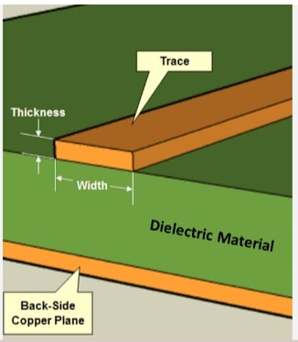
Trace cross-sectional area
The cross-sectional area is directly proportional to the current-carrying capacity. It means more surface area, more heat dissipation, and incidentally more current-carrying capacity. Now, the cross-sectional area is based on trace thickness and trace width. Altering trace thickness is not always feasible due to manufacturing limitations. Hence, to achieve a proper current rating, we can increase the trace width. The trace surface area will act as a heat sink. When there is a 10℃ temperature change, a thicker trace can handle the sudden change in current more effectively than a thinner one (as mentioned in the equation earlier, a change in temperature will lead to a change in the current). But in certain situations, a shortage of space resists the increase in trace width. In that case, we can increase the trace thickness by soldering on the top of the trace.
Why should we calculate the current in vias?
The size of vias is one of the critical factors to achieve the required current rating because they have resistance values. We know resistivity is inversely proportional to conductivity, so larger vias have lower resistance and vice versa. Resistance in vias causes heat dissipation.
If vias are designed without considering the required current rating, the trace could be burned out, and the risk of high voltage drop could arise.
In 2009, IPC developed IPC-2152 ‘standard for current carrying capacity in printed board design’. It helps to fix the appropriate sizes of internal and external conductors based on the required current rating and allowable temperature rise over ambient. Our case study on designing a high-current PCB with voltage doublers demonstrates how we implemented via stitching by determining the current-carrying capacity of a single via.
IPC 2152 standard
IPC-2152 replaces the 50-year-old IPC-2221B standard. IPC-2221B determined the connection among temperature rise in PCBs, current in the trace, and the trace cross-sectional area in a series of charts when there was no multilayer board.
IPC-2152 establishes the outline of how thermal conductivity, vias, board material, and thickness are related to current, trace cross-section, copper weight, and temperature. It also ascertains the accurate values for external and internal traces. IPC -2152 is not only a real-time-saver but also helps PCB designers to model a safe and appropriate design. Sierra Circuits Trace Width and Current Capacity calculator is based on this standard. You can calculate the trace area and current capacity for a certain temperature rise. You can find more about it in the sections below.
Measures to regulate the current carrying capacity
Taking proper measurements to control the current-carrying capacity of vias at the very beginning of PCB design ensures proper functionality and performance. Here are some golden rules to regulate the current rating.
Via fabrication
While fabricating vias, three critical factors to be considered are the via hole inner diameter, the hole wall thickness, and the pad annular ring. As mentioned earlier, vias and microvias are made conductive by electroplating holes. The thermal conductivity of vias is increased by tenting, plugging, or filling.

Design for Manufacturing Handbook
11 Chapters - 96 Pages - 90 Minute ReadWhat's Inside:
- Annular rings: avoid drill breakouts
- Vias: optimize your design
- Trace width and space: follow the best practices
- Solder mask and silkscreen: get the must-knows
Download Now
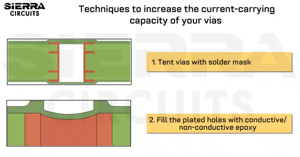
Via tenting
Tenting of a via is actually covering the annular ring and via hole with a solder mask. It protects the copper traces from corrosion, oxidation and reduces the risk of shorting in the circuit.
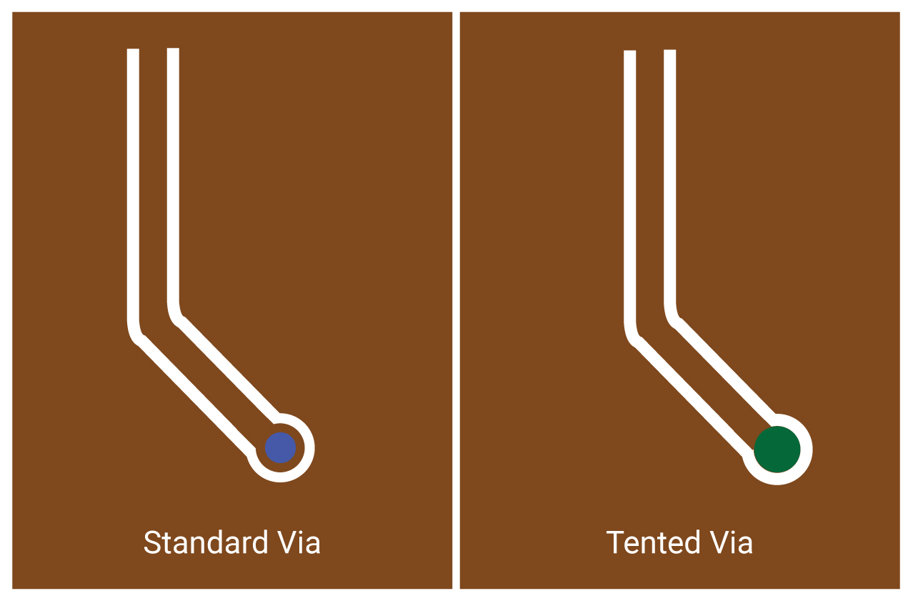
Brown: Copper layer
Blue: Drill layer
Green: Solder mask layer
Via plugging
Via plugging is a process where vias are filled with epoxy resin and closed with a solder mask. It can be accomplished by using conductive or non-conductive materials. The use of conductive filling in vias can increase the capacity to carry current from one layer to another.


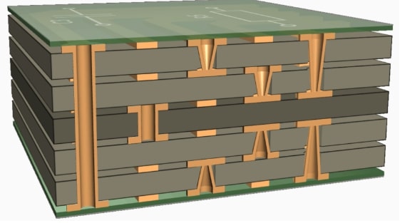
Multilevel optimized interconnection
In this process, we are used to making a strong vertical connection between layers. Routing high current always involves using as much metal as possible to reduce the heating effect as well as to lower inductance. It is a technique where multiple vias are used on different layers of conductive material and then connected. Microvias, buried vias and blind vias are most effectively used to mitigate unnecessary parasitic inductance and capacitance. In this regard, one keynote can be mentioned that a shorter length of interconnection reduces unwanted stub impedance. Therefore, the current carrying capacity is elevated. To learn the effects of via impedance discontinuity, see how via impedance impacts signal integrity in pcbs.
Trace width calculator
A recent article by Douglas Brook and Johannes Adam, “Vias Are Cooler Than We Think” in ‘Signal Integrity Journal’, presents some experimental results and respective measured values. The tables show the effect of temperature and trace width on current-carrying capacity.
Via temperature using simulation method
Trace width (mils) Current (A) Trace temperature (℃) Via temperature (℃) Via T/ Trace T
27 4.75 72.8 70.1 96.3
27 6.65 114.2 108.2 94.7
200 4.75 30.8 31.8 103.2
200 8.55 44.8 48.1 107.4
Measured results of via tests
Trace width (mils) Current(A) Trace temperature (℃) Via temperature (℃) Via T/Trace T
27 4.75 66 64.5 97.7
27 6.65 114 109 95.6
200 4.75 30.5 31.5 103.3
200 8.55 40.5 44.5 109.9
For high-current PCBs, trace width calculation is crucial. From the above tables, we can evaluate the current carrying capability of a specific trace width. Via is considered as a cylinder of copper and its circumference is 2𝝅r or 𝝅d, where d is the size of the via hole. The circumference will be analogous to the trace.
Sierra Circuits’ Trace Width calculator
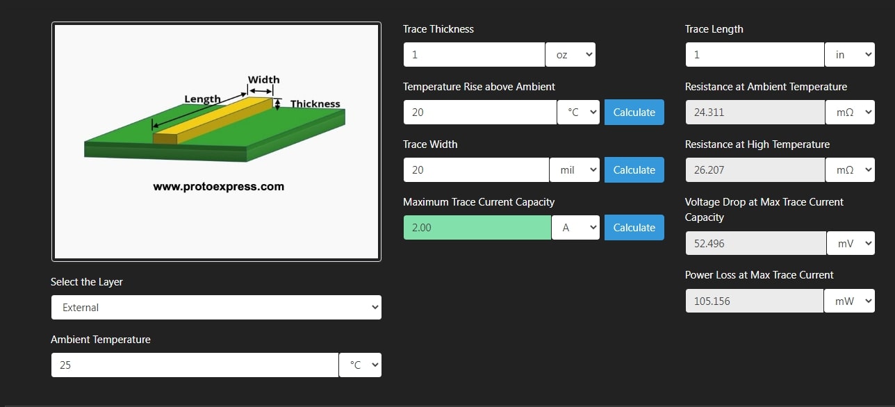
Sierra Circuits provides a three-in-one trace width calculator that can calculate trace width, amount of trace current, and temperature rise. Changing any two parameters, we can get the value of the third one for a given trace thickness. Additionally, it can also give the values of DC resistance and the voltage drop across a trace of a given length. The default values for trace length and ambient temperature are 1 inch and 25℃, respectively. The values can be changed as per requirement. The tool has the flexibility of using different units. Sierra Circuits’ Trace Width calculator is based on the recent IPC-2152 standard.

Sierra Circuits’ Via Current Capacity Calculator
As per IPC-2152, the cross-sectional areas of the via and the trace should be the same. The factors that are responsible for trace current also have a major role in determining the via current. But we know the plating of a via is different from that of a trace. Hence, precision and proficiency are paramount in via current calculations to evade degradation in PCB performance.
Sierra Circuits has launched a Via Current Capacity and Temperature Rise calculator to help designers create perfect PCB vias. This tool determines via diameter, current carrying capacity, and temperature rise over ambient. The standard values for input parameters like height and plating thickness of via are available in the help section. You can use different units for each parameter at your convenience. Designers can also find important parameters like resistance, voltage drop, and power loss for a particular current rating here.
Other factors that influence via current capacity
From the above-mentioned facts, we can see that primarily, the cross-sectional area and temperature are the factors that determine current carrying capacity. But there are other elements too that can impact the capacity.
- Vias are connected to traces; if the trace is not wide enough, a spike of current could burn the trace or via. It is due to uneven soldering which increases the cross-sectional area while the trace width remains the same.
- To avoid overcurrent issues, designers should consider having a clean board free from contaminants. The contaminants and dust particles also affect the current carrying capacity.
- In high current flow, curved traces with acute angles can have an adverse impact on carrying current. Though it is not a major issue in low-current transmission.
- PCB base material is also important in this regard. A trace of the same thickness and width but with different base materials can greatly affect the current-carrying capacity of vias. It is due to the different thermal conducting characteristics of different materials.
Vias transfer electrical signals in a shorter path from one layer to another and can undergo signal integrity issues. Hence, efficient and appropriate calculation of the current rating and imposing the right design constraints are necessary for designing them to eliminate the risk of damage and degradation of the circuit.
You can book a meeting with our experts or call us at +1 (800) 763-7503.

About Poulomi Ghosh : Poulomi is a microwave engineer specializing in EMI, EMC, RF, and high-speed electronics. As a senior technical writer at Sierra Circuits, she creates advanced engineering articles and webinars for hardware engineers and PCB designers.


