What is silkscreen in a PCB?
PCB silkscreen provides text-based information of different circuit points, components, and other circuitry information as per requirement. Silkscreen marking consist of:
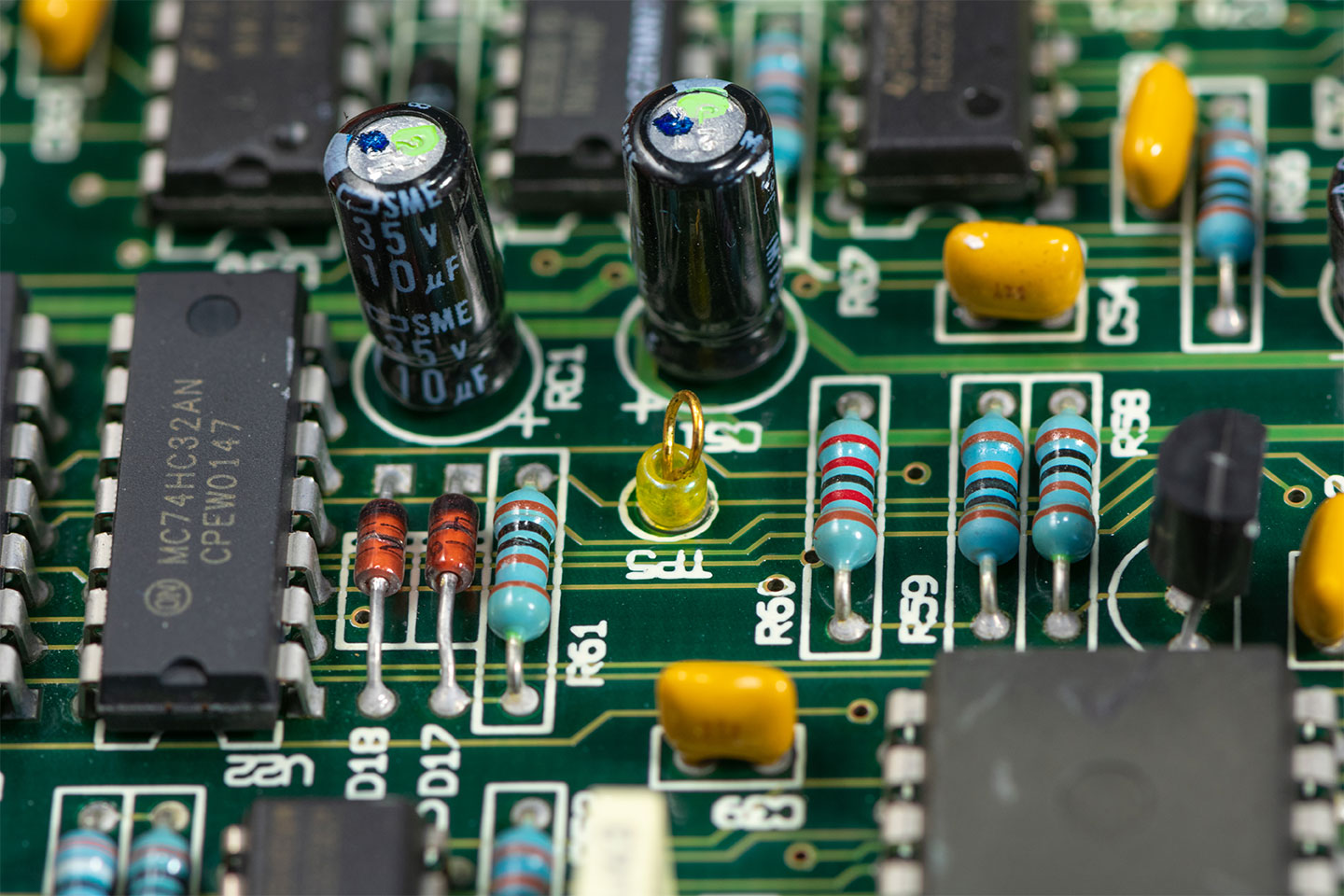
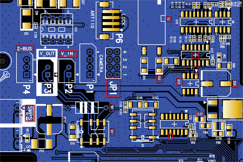
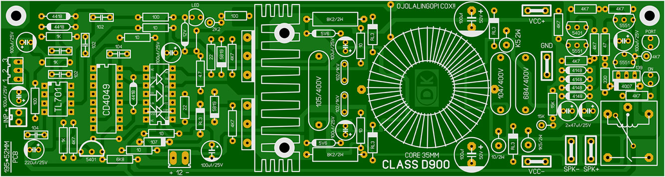
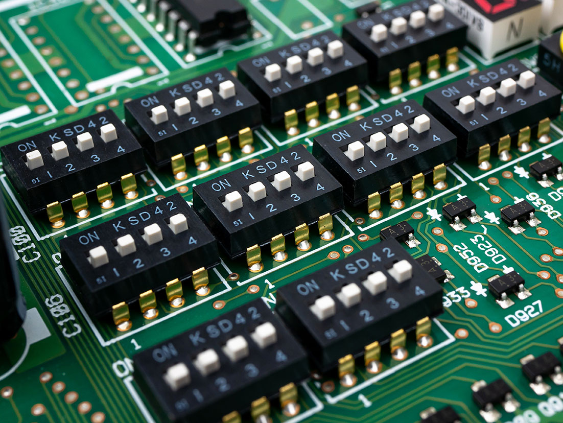
- Component reference designators
- Polarity marking
- Pin 1 marking
- Component boundaries
- Company logos
- Manufacturer marks
- Warning symbols
- Part numbers
- Version numbers
- Date code
Silkscreen information varies according to the size of the circuit boards. The most critical information should be prioritized if you have limited space.
Design considerations for PCB silkscreen
Silkscreen layout aids in the assembly of a circuit board by providing reference designators. A few parameters for designing are listed below.
Component orientation marking
The orientation marking on the silkscreen gives the direction in which the component is soldered. These are typically represented by a dot(.). It indicates pin no.1 of the IC, “(+ or –)” in the case of diodes and LEDs, (C) for cathode, and (A) for anode. In the case of a capacitor half-shaded circle for negative and “+” for positive polarity.
Silkscreen printing process
It is essential to find out the specific method that a board manufacturer implements for silkscreen printing. The printing method influences many design parameters such as size, clearances, and location of silkscreen markings on different elements, such as component pads, traces, and vias. These parameters are specified according to manual silkscreen printing, liquid photo imaging, and direct legend printing.

Design for Manufacturing Handbook
11 Chapters - 96 Pages - 90 Minute ReadWhat's Inside:
- Annular rings: avoid drill breakouts
- Vias: optimize your design
- Trace width and space: follow the best practices
- Solder mask and silkscreen: get the must-knows
Download Now
Silkscreen checks for PCB layout
While designing a PCB layout, markings such as polarity, pins, and reference indicators must be close to the associated components and should be visible after component mounting. This is done to ensure there is no overlap or covering of the indicators.
Appropriate fonts
Some circuit board manufacturers allow the designer to create any type of font style for the silkscreen. However, it is best to consult with the fabricator about the kind of font that can be generated on the board. Later, the appropriate font should be incorporated into the design. Designers should mention the requirements for silkscreen printing such as size, height, color, and font type. The most common sizes are 35 mil height and 5 mil line width and also 25 mil height and 5 mil line width.
Proper use of silkscreen markings
It may be fascinating to include indicators for all components and other informational imagery that may be useful for assembly, testing, or repair of the board. However, with the ongoing development toward smaller PCBs, this may not be possible. Thus, it is critical to prioritize the marking as given below:
Regulatory requirements: It involves marking and labeling of components to identify lead (Pb), lead-free (Pb-free), and other attributes from IPC.
Manufacturer’s identification: It includes markings such as board pad number, serial number, labels, and the logo.
Assembly aids: It involves polarity and pin one indicator. Reference indicators should be used according to the available space.
Testing aids: It includes test point indicators, mode, and jumper indicators.
Additional design considerations
There are some more points to be considered while designing the silkscreen, they are:
- For easy readability, marking should be done using standard colors (white color is widely used) and proper shapes.
- To reduce the problems occurring due to machine printing errors, tolerance should be presented by a few mils difference.
Finally, the best pattern for the silkscreen can be achieved by following these guidelines.
How do you screen print a PCB?
The screen printing process involves a screen formed by stretching a mesh of fine polyester or stainless steel wires over a rigid frame to serve as an image carrier. A stencil of the required image is created by applying a photosensitive emulsion to the mesh. The emulsion is usually applied on both sides of the mesh, and a defined thickness is built upon the underside (the side that contacts the board).
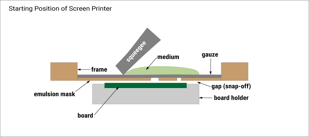
As shown in the figure, the screen is positioned just above the board, and the medium (ink) lies in front of a flexible squeegee. While the squeegee moves across the screen, the mesh of the screen comes in contact with the board, allowing the medium to roll onto the PCB.
Initially, the squeegee blade presses the medium into the open apertures of the image, and then removes the excess as it passes through each aperture. In this process, the mesh aperture on the screen is pulled away from the printed surface behind the squeegee, leaving behind the ink that was once inside the mesh aperture. The medium flows slightly after printing to reduce visible mesh marks left in the print. This process is called leveling.
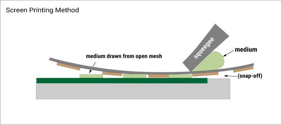
Since the screen comes in contact with the surface when the squeegee passes over it, this process is sometimes referred to as off-contact printing. For each 100mm of frame width, the snap-off distance is typically 0.5mm. The thickness of the deposited ink is determined by the total thickness of the emulsion and the mesh.
Methods for creating a silkscreen
There are mainly three silkscreen methods:
- Manual screen printing
- Liquid photo imaging
- Direct legend printing
There are various factors to consider while choosing the silkscreen method including time, cost, the level of precision required, the level of spacing available, and the material used.
Manual screen printing
Manual screen printing is the conventional and economical method of printing. This process is carried out using epoxy ink. The ink is applied to the laminate and dried to obtain the impression on the board.
It is easier to set up manual printing. Moreover, it is also a cost-effective option. However, there are downsides to this method such as the large spacing required between boards and the impression drying time. This is because of the larger text size supported by this method. The pad clearance is another challenging factor.
When costs are low and board spacing is not a concern, you should consider manual screen printing.
Liquid photo imaging
In liquid photo imaging, the laminate is first coated with epoxy. Then it is exposed to UV light to obtain the image. The results of liquid photo imaging are more precise than those of manual silkscreening. Furthermore, this method uses the board space more efficiently by reducing the required spacing.
The ink used in this process is higher compared to the other two. It also requires more time for setup along with the application time.
A liquid photo imaging system will let you save space on your board as well as provide fine resolution.
Direct legend printing
Direct legend printing (DLP) uses high-end inkjet printers that have the ability to apply ink to circuit boards. In this process, CAD application data is directly printed on the PCB. Direct legend printing uses acrylic ink to save drying time. This method has the highest accuracy and best time efficiency. It can accommodate a very low text height, but lower than 0.02 inches is not recommended as it will not be readable.
A DLP system offers benefits in terms of time and board spacing. But this is an expensive method. Hence, it is necessary to consider all these things and select the method accordingly.
Silkscreening a PCB is a delicate process that can enhance the quality of your board, and also adds value through a classy design.


