PCB backdrilling process is a critical manufacturing procedure that reduces signal reflections due to conductive via stubs. High-speed board design poses several challenges in terms of retaining signal integrity, which can be resolved through proper design and manufacturing practices.
Via stub which is a non-functional part of a via, causes significant signal integrity issues in high-speed design. These stubs lead to signal reflection from the stub end, and this reflection will interfere with the original signal. To resolve this, a manufacturer can employ back drilling, where most of the via stub is removed by re-drilling with a slightly larger drill bit.
Beat competitors to the market. Reduce Respins with our Zero-Defect Guarantee.
With Turnkey PRO, Sierra Circuits delivers full turnkey PCB assemblies guaranteed to work.
What is the PCB backdrilling process?
Back drilling involves drilling a hole slightly larger in diameter than the PTH to remove the conductive via stub.
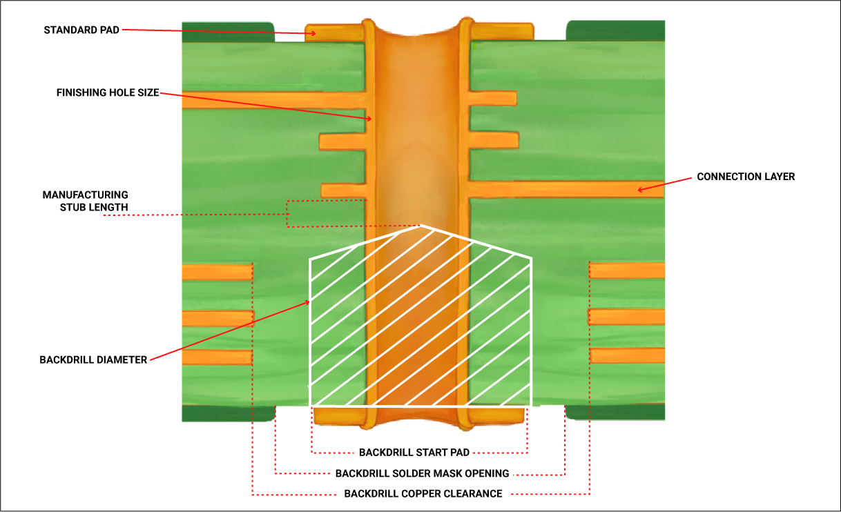
Back drilling or controlled depth drilling (CDD) is a method used to remove the unused portion or stub of the copper barrel from a through-hole via in a PCB. Since such holes are back-drilled to a preset and controlled depth, this type of drilling is also known as controlled depth drilling. Ideally, the via stub left after this procedure should be smaller than 10 mil.
The table below provides a quick reference for backdrill clearances and drilling tolerances.
| Parameter | Recommended values |
|---|---|
| Back drill to copper clearance | 10 mil |
| Back drill to back drill clearance | 6 mil |
| Min. back drill oversize diameter | 8 – 10 mil |
| Min. depth for controlled depth drilling | >1 mil |
| Controlled depth drilling tolerance | ±2 mil |
Also, see PCB milling to learn how slots, cut-outs, cavities, and board outlines are formed during fabrication.
Steps involved in the backdrilling process
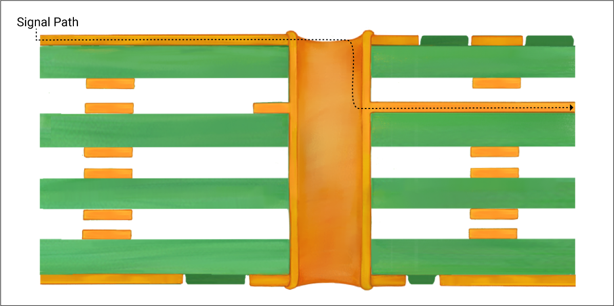
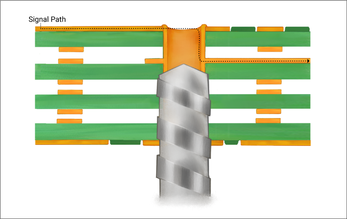
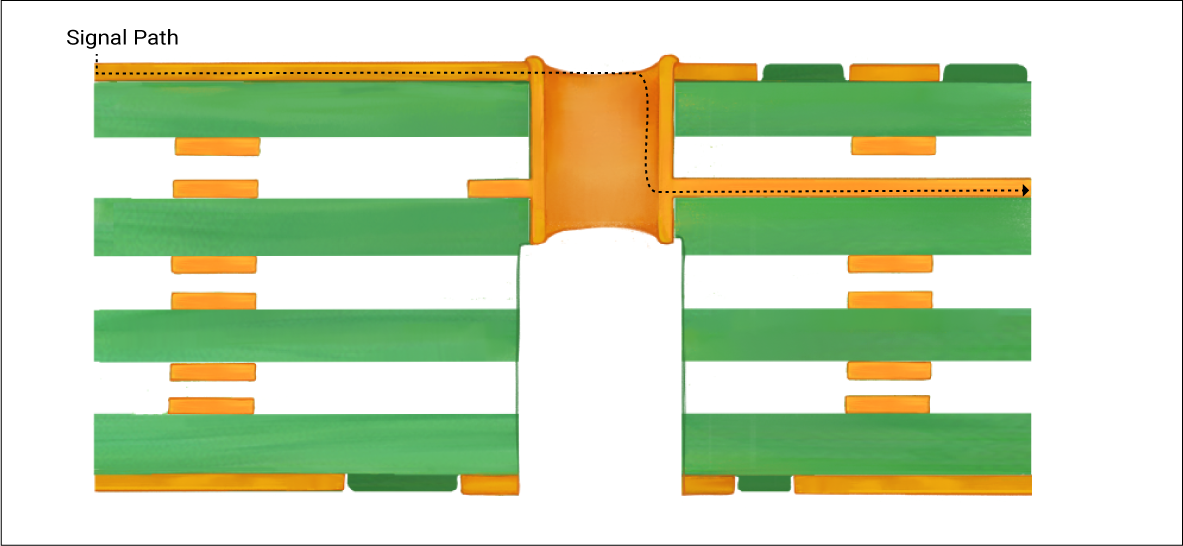
The images given below illustrate the steps involved in CDD.
- The first step is to identify the via stub extending beyond the signal path in the board.
- The second step involves back drilling using a drill bit with a slightly larger drill diameter.
- After the removal of via stub through CDD and finishing, it will look like the figure given below:
Discover the essential PCB mechanical processes that shape and prepare circuit boards for assembly.
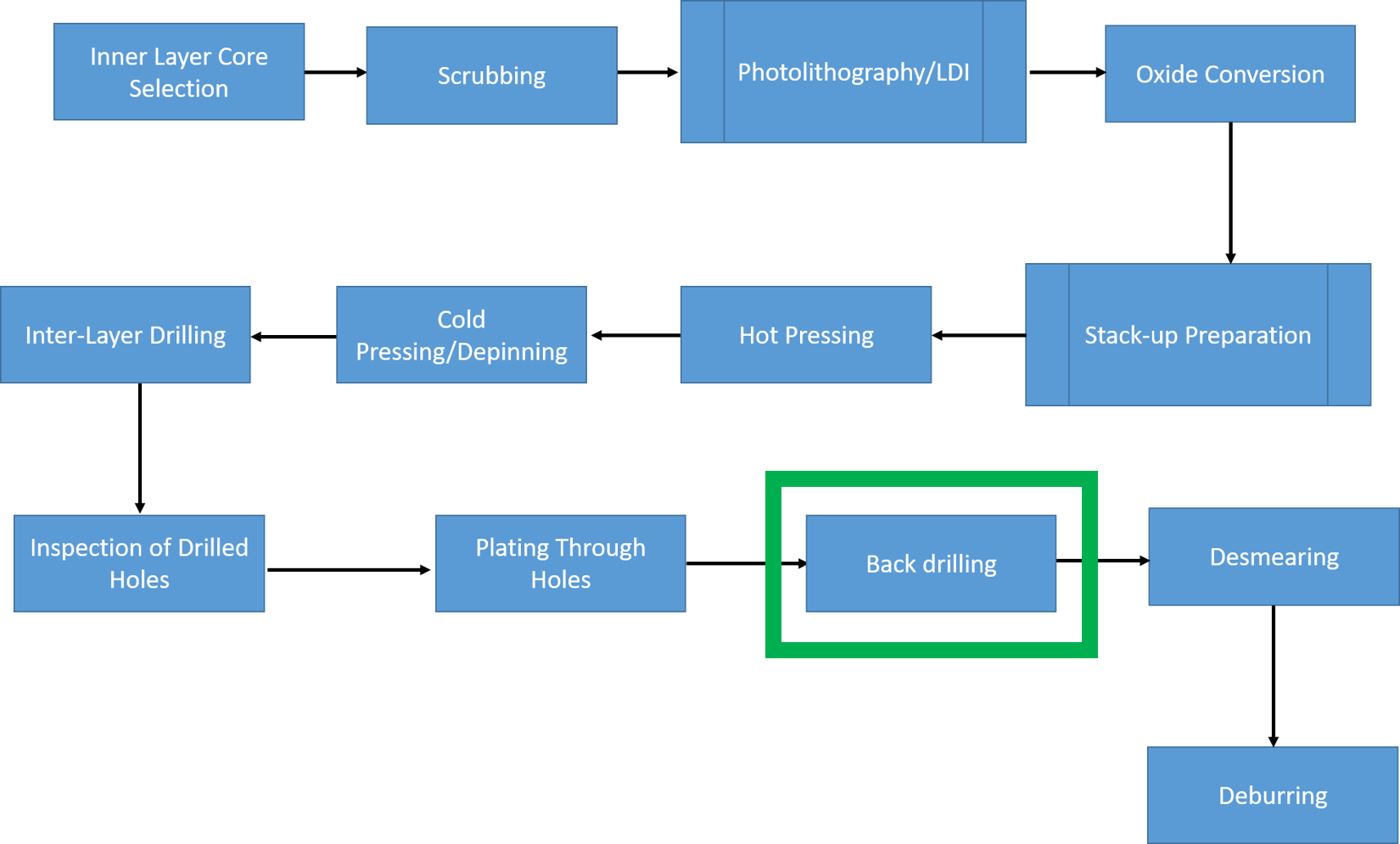
Where does back drilling fit into the PCB design and development process?
Control depth drilling is done right after the PTH process and before the desmearing process. This is because the holes need to be plated to conduct signals, and it becomes challenging to carry out this process after backdrilling. The process flow given below shows you the steps that occur before and after the backdrilling process.
Sierra Circuits’ engineers and technicians have the experience to bring your PCBs to life.
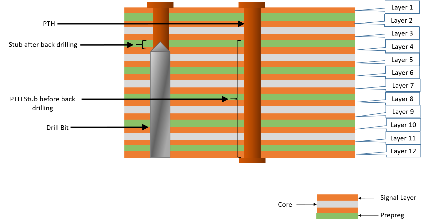
Controlled depth drilling example
To explain the process of backdrilling, we can consider a 12-layer PCB with a through-hole via passing from layer 1 to layer 12 in a 12-layer stack-up. The requirement for signal transmission is only from layers 1 to 3, leading to the creation of a via stub from layer 3 to layer 12, causing signal reflections and resonance at high frequencies. At the resonant frequency, the signals get attenuated, which is undesirable. Therefore, back drilling is implemented here to remove the copper plating from layers 3 to 12, minimizing the stub length. One condition that needs to be met in this process is that the back drill diameter needs to be slightly bigger than the original hole size to remove the unwanted copper plating.
Explore best practices and common techniques for drilling and plating through holes in multilayer PCBs.
Advantages of back-drilling PTH vias
- Decreasing the deterministic jitter by back drilling will significantly reduce the comprehensive BER (bit error rate) of the signal. The BER is the number of bit errors per unit time and is largely dependent on deterministic jitter. Via stubs give rise to a signal distortion issue named deterministic jitter. Jitter with respect to signal transmission in a circuit board refers to timing errors caused by EMI, noise, and signal crosstalk. Deterministic jitter is the jitter that can be defined within the minimum and maximum variations.
- Minimizes signal attenuation due to enhanced impedance matching and reduces EMI/EMC radiation from the stub
Backdrilling is one of the many manufacturing practices to ensure signal integrity in a board design. PCB designers need to work along with manufacturers to identify where this process can be applied to minimize signal reflections and boost signal integrity.
[design_guide id="309"]
Try our free Better DFM tool and save time and money. Our automated platform will catch any PCB design error ahead of time and prevent on-holds and re-spins.
Get started by uploading your Gerber files here.


