There is a huge demand for the replacement of tin-lead (Sn/Pb) solders with lead-free solders in the electronics industry because of health and environmental concerns. Lead-free HASL is a popular finish that provides the most durable finish for PCBs.
What is lead-free HASL PCB surface finish?
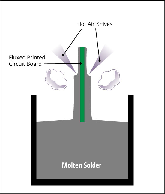
Lead-free HASL is a type of surface finish that uses lead-free alloys instead of tin-lead (Sn-37Pb) eutectic alloys. Initially, molten solder is applied on a board (after cleaning and fluxing) to achieve wetting and excess solder is scraped with the help of air knives (a tool that is set at a temperature above the melting point of the solder). After the solder solidifies, the circuit board is passed through the washer where the solder flux residues are removed.
There are two methods of applying lead-free HASL:
- Vertical process: Vertical process involves a panel of boards mounted on a frame that moves vertically downward into the solder bath, holds for a certain time (usually 2-3 seconds), and then lifts the panel through the operating air knives. These knives are adjusted to clear through-holes and vias while leaving a sufficient thickness of solder on all areas where a solderable finish is essential. After the solder cools and solidifies, the panel passes through the washer/dryer to remove flux residues. The operator then inspects the quality of the finish.
- Horizontal process: In the horizontal process, the board is flooded with solder applied through nozzles or between rollers on the top and bottom of the panel before being moved between hot air knives placed above and below the panel.
Usually, HASL lines are of vertical design and deliver a high-quality finish. Fully automated vertical lines can deliver rack-to-rack performance including fluxing, preheating, washing, and drying. The finish in the horizontal process is more uniform in thickness compared to the vertical process.
The lead (Pb) level in lead-free solder is less than 0.1%. Castin (a composition of Sn 93 98%, Ag 1.5-3.5%, Cu 0.2-2%, and Sb 0.2-2%) alloy and SnCu 0.7 are widely used in this process.

Design for Manufacturing Handbook
11 Chapters - 96 Pages - 90 Minute ReadWhat's Inside:
- Annular rings: avoid drill breakouts
- Vias: optimize your design
- Trace width and space: follow the best practices
- Solder mask and silkscreen: get the must-knows
Download Now
Why is lead-free HASL used?
There are several problems associated with the HASL process as given below:
- Damage due to additional thermal deviations
- Coplanarity issues because of pad to pad variation in coating thickness
- Stencil gasketing issue related to the difference in coating thickness and mushroom cap profile (of the coating) found on small pads.
- Heat and fumes associated with the process were considered out of place in modern board shops.
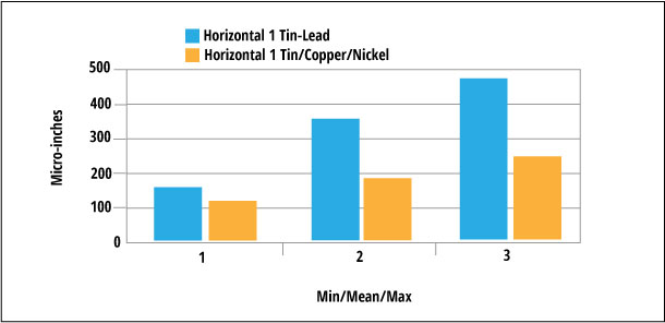
The difference in the solder coating thickness of a lead-free HASL finish is usually about half that of the tin-lead HASL finish. The coplanarity is also good in this finish. The modern HASL line is designed to provide the operating conditions in line with other equipment in modern board shops to avoid issues with heat and fumes.
Coating thickness
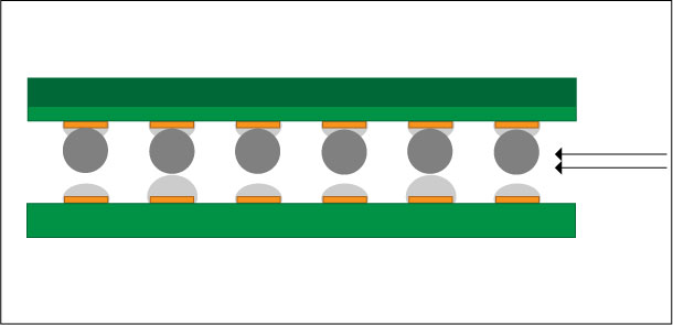
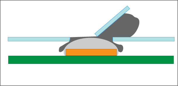
The solder coating profile is defined by the volume of solder left on the pad after passing the board through the hot air knife and surface tension forces. Due to surface tension, the coating has a tendency to be thicker on smaller pads.
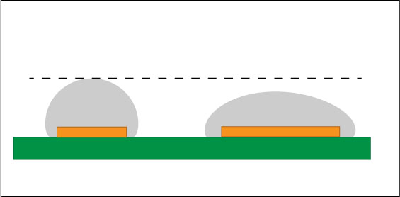
Because of the higher surface tension of lead-free solder, the coating formed in the HASL process is both thinner and uniform compared to tin-lead solder formed in similar conditions.
The coating thickness can be checked by XRF (X-ray fluorescence spectroscopy) technique.
Whisker formation
Compressive stress is the driving force for whiskers (a thin filament protruding from a board surface having tin as a final finish). According to the JESD22A121 specification, whiskers appear on the hot-dipped lead-free finish on copper only in areas where compressive stress is intentionally introduced and under the most severe conditions such as the combination of elevated temperature (60°C) and high humidity (87%RH).
Lead-free HASL provides a corrosion-resistant finish that can assure solderability over long periods.


