What is solder paste?
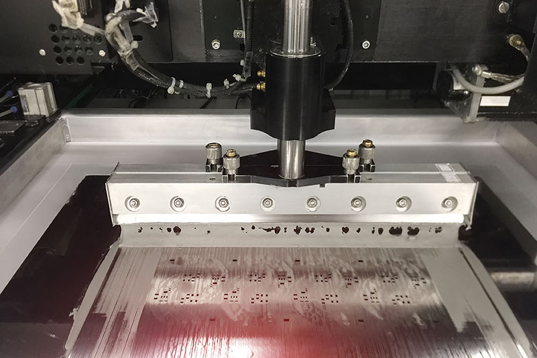
Solder paste is a combination of powdered metal solder and flux medium. It is applied on a PCB with the help of a stencil or a foil. A stencil is a thin sheet of material (usually stainless steel) with a series of apertures (holes) cut into it that resemble the component pads on the board.
The stencil accurately deposits the right amount of paste on surface mount pads. It should be properly aligned on the circuit board. Solder paste application is one of the most important aspects of surface mount assembly.
How many types of solder paste are there?
They are classified into three main types, as given below:
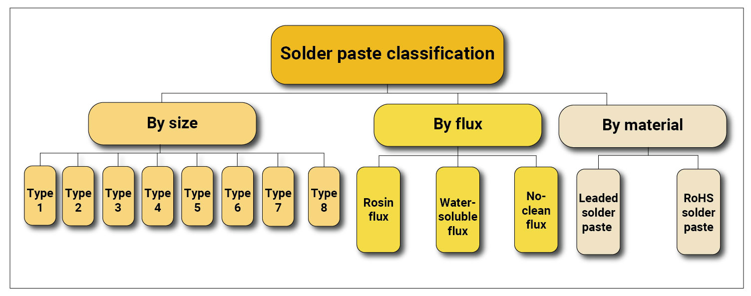
Based on the particle size as per IPC J-STD 005 standard
| Type designation | Particle size in µm |
|---|---|
| Type 1 | 150-75 |
| Type 2 | 75-45 |
| Type 3 | 45-25 |
| Type 4 | 38-20 |
| Type 5 | 25-10 |
| Type 6 | 15-5 |
| Type 7 | 11-2 |
| Type 8 | 8-2 |
Based on the flux type
Solder paste is classified into three main types according to the flux type.
Rosin flux is made from rosin and withstands high soldering temperatures. It forms a barrier against moisture. Rosin flux has low activity and is suitable for surfaces that are clean and easy to solder.
Water-soluble flux contains organic acids, thixotropic, and solvents. Its activity levels vary from no activity to extremely high, and it can also solder difficult surfaces. Since it covers all the activity levels, product specifications should be considered according to corrosion and electrical conductivity hazards.
No-clean flux consists of rosins, solvent, and a small portion of activator. It has a low to moderate activity and is suitable for easily solderable surfaces. This flux eliminates the need for cleaning the residues formed after soldering.
Based on material
- Leaded solder paste: It consists of a metal alloy with lead and tin as its base constituents. This solder is affected by environmental conditions.
- RoHS (lead-free) solder paste: It is a composition of various elements such as copper, tin, silver, nickel, zinc, bismuth, and antimony. RoHS is environment-friendly.

Soldering Flux eBook
13 Chapters - 24 Pages - 40 Minute ReadWhat's Inside:
- Why flux is needed
- The ingredients of flux and what they do
- Soldering flux categories
- How to read a flux manufacturer’s technical data
- The best flux for various applications
Download Now
Solder paste application key considerations
Stencil thickness
Stencil thickness ensures that the correct volume of solder paste is properly released from the apertures to achieve the required solder joint.
If the stencil is too thick, the paste may be held to the inner walls of the aperture by surface tension.
The following formula can be used to select the proper stencil thickness:
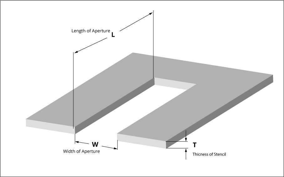
Aspect ratio = Aperture width/stencil thickness
Area ratio = Area of the pad (L × W)/ Area of aperture walls (2 × (L+W) × T)
Aperture design
Aperture design is important to prevent the formation of solder defects (bridging and solder beads). Mostly, apertures are designed to be a bit smaller than the pads to provide a good gasket seal between the stencil and the circuit board. However, some apertures require a special design to deposit less paste on the inner edge of the part to reduce the formation of mid-chip solder balls.
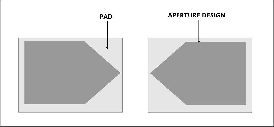
Refer to the IPC standard while defining the surface mount pad dimensions.
Stencil material and mounting
The stencil’s material influences its potential to release the solder paste from the apertures. Stainless steel is commonly used; however, for fine pitch devices, a more expensive option like nickel is implemented.
A multilevel or stepped stencil can accommodate both fine-pitch devices that require a thin stencil and also larger parts that require a thick stencil.
Step-up areas are produced by adding material to the stencil to increase the volume and height of the solder paste in chosen areas. Step-down areas are produced by removing material from the stencil to reduce the volume and height of the paste deposition in selected areas.
Stencil alignment
Accurate alignment of a stencil is crucial for printing the solder paste onto the pads. It is attained by adding registration marks known as fiducial marks to both the PCB and the stencil.
The diameter of fiducial marks should be between 1 to 3 mm.
A minimum clearance of at least 3 mm should be there from the board’s edge. This is to ensure that these marks are not getting covered by conveyors or automated placement machinery/tools.
- For best accuracy, 3 global fiducials should be placed on the board’s edges.
- At least 2 local fiducials should be diagonally placed on the outside of the surface-mount component.
Solder paste stencil design specifications
Circuit boards with copper pads that promote conductivity and heat dissipation require uniquely designed stencils. For thermal pads, stencils use a windowing effect so that the excess solder does not deposit on the pads. This is achieved by designing a window effect in the stencil.
Pin-in-paste soldering (PIP)
Traditionally, through-hole components are soldered on PCBs by inserting their leads into holes and then soldering them from the opposite side. Often, this creates solder bridges in your board.
To mitigate this challenge, we implement pin-in-paste soldering. This technique allows through-hole components to be reflow soldered like surface mount components. Unlike others, this soldering method maintains a stable temperature during PCB assembly.
Step-by-step process of pin-in-paste soldering

- Panel preparation: Solder paste is applied to the pads using a stencil.
- Pre-trimmed PTH component insertion: The through-hole components are inserted into the pre-applied solder paste on the PCB surface. The paste acts as an adhesive and holds the components in place.
- Reflow soldering: During this step, the PCB is subjected to a controlled temperature to melt the solder paste and form a reliable electrical connection. The surface tension of the molten solder ensures proper wetting and bonding between the components and mounting holes.
- Cooling and inspection: After reflow, the board is cooled naturally before inspecting for defects, such as solder bridges and insufficient solder joints. For thorough quality assurance, we run an X-ray inspection.
Advantages of PIP
- PIP eliminates the need for separate wave soldering for PCBs with SMDs and through-hole components.
- As pin-in-paste requires less space than manual soldering, it enables tighter component placement, which is ideal for HDI designs.
- The solder joints formed through pin-in-paste soldering typically exhibit better mechanical strength and reliability than traditional wave soldering methods.
Disadvantages of PIP
- Not all through-hole components can withstand PIP’s reflow temperatures.
- Compared to wave soldering, PIP requires stringent inspection due to smaller solder joints.
- Stencils and specialized equipment can add to the overall cost.
Weighing the advantages and disadvantages alongside, you can determine if PIP is the right soldering technique for your next project.


