


Contents
IPC-2221 serves as the foundational standard for PCB design, covering electrical spacing, material selection, conductor sizing, and verification. It ensures electrical safety, manufacturability, and reliability across various PCB technologies.
You can use IPC-2221 to define conductor spacing, creepage/clearance, insulation, and trace dimensions early, complemented by IPC-2220 standards such as IPC-2222 for rigid boards, IPC-2223 for flex circuits, and IPC-2226 for HDI designs to address technology-specific constraints.
IPC-2221 establishes standards for PCB design aspects such as schematic, material selection, thermal management, DFM, DFA, DFT, and quality assurance. Some of the primary design requirements of high-voltage boards are defined in IPC-2221B. They include conductor spacing, creepage, and insulation requirements. Before diving into the details, let’s have a look at IPC standards in general.
Highlights:
- Start every PCB design with IPC-2221, then apply the correct IPC-222x sectional standard based on board type (rigid, flex, HDI, PC card, or MCM-L).
- Do not rely solely on IPC-2221 minimum spacing for high-voltage designs; increase clearance and creepage using slots, barriers, layer separation, and board-side partitioning.
- Implement standardized E-coupons and H-coupons to validate surface and bulk insulation resistance.
- Select insulation materials using CTI ratings, not just dielectric constant, when designing for elevated voltages or contaminated environments.
What are IPC standards?
IPC standards are globally recognized guidelines developed by the Global Electronics Association (formerly IPC – Institute of Printed Circuits) that define best practices for PCB design, materials, assembly, inspection, and performance. By standardizing technical requirements across the electronics supply chain, these standards reduce ambiguity between designers and manufacturers and help achieve consistent quality and high-yield production.
Why is the IPC-2221 standard important for PCB design?
IPC-2221 defines the generic design requirements for organic printed circuit boards, serving as the foundational guideline for building reliable circuit boards. It covers essential aspects such as:
- Component placement, interconnection structures.
- High-voltage electrical considerations (including conductor spacing, PDN bus layouts, controlled impedance, heat dissipation, and test coupon design).
- Material selection using organic or mixed organic–inorganic substrates.
As the core document in the IPC-2220 series, IPC-2221 establishes baseline rules that are further refined by standards tailored to specific board types such as rigid, flex, and HDI PCBs.
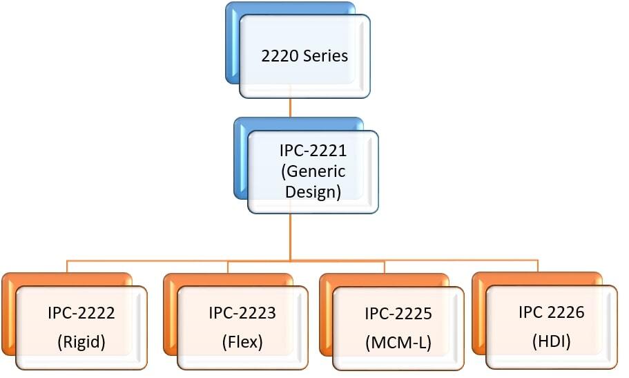
How do IPC-2220 series standards apply to different PCB types?
The IPC-2220 series follows a hierarchical structure. The IPC-2221 serves as the foundational design standard for all board types. The image below describes how the benchmark caters to all types of boards.
Always use the IPC-2221 in conjunction with the detailed requirements specific to your design and board type. For instance, rigid PCB designs require compliance with the generic requirements of IPC-2221 along with the additional rules defined in IPC-2222.
IPC-2222: sectional standard for rigid boards
The standard mentions the optimized rules for efficient component placement, routing density, and superior electrical performance to achieve a flawless design. Used in conjunction with IPC-2221, IPC-2222 sets standards for the following factors to increase the manufacturability of a rigid circuit:
- Holes and interconnections specifics
- Dielectric spacing
- Selection of materials
- Routing parameters
- Board thickness tolerance
- Mechanical parameters
IPC-2223: sectional standard for flex circuits
The key design considerations, mentioned in IPC-2223, for designing a perfect flex board, are listed below:
- Material selection and construction
- Selective plating
- Minimum bend radius for flexible circuits
- How to achieve controlled impedance
- Unsupported edge conductor design
- Filling of via
- Pad placement
IPC-2224: standards for designing PWBs with PC Cards
It is a set of requirements for designing PC cards. The standard also guides you to secure passive and active components such as through-hole, fine-pitch BGAs, unpackaged bare die, array mount, and surface mount devices. The material specifications ensure faultless physical, thermal, and electrical functions of the following types of boards:
- Type I: Single-sided circuit board
- Type II: Double-sided circuit board
- Type III: Multilayer board without blind or buried vias
- Type IV: Multilayer board with blind or buried vias
- Type V: Multilayer metal core board without blind or buried vias
- Type VI: Multilayer board with metal core and blind or buried vias
IPC-2225: designing organic multichip modules (MCM-L) and MCM-L assemblies
It establishes the regulations for designing and assembling bare chips on the substrate. This incorporates adhesive details, attached dies, and microvia materials.
IPC-2226: standards for designing HDI boards
The benchmark defines the requirements for HDI structures. It provides attributes for power, ground, signal, and combined layer details, information on dielectric separation, via formation, and other crucial factors of the HDI substrate.
The classification is based on the number and location of the circuit layers that may or may not connect to the substrate.
It classifies HDI boards into six industry-accepted categories.
- Type I (1 [C] 0 and 1 [C] 1): Through vias connecting the outer layers.
- Type II (1 [C] 0 or 1 [C] 1): Buried vias in the core and may have through vias connecting the outer layers.
- Type III ( ≥ 2 [C] ≥ 0 ): The core may have buried vias or through vias connecting the outer layers.
- Type IV (≥ 1 [P] ≥ 0): Here, P is a passive substrate with no electrical connection.
- Type V: Constructions without a core.
- Type VI: Other constructions.
The [C] symbol is used if the layers are adjacent to the core. For passive connections, [P] is implemented.
For instance, an HDI board with two layers on one side of the core and one layer on the opposite side can be represented as 2 [C] 1.

Fill out the form:
Why is IPC-2221 significant for high-voltage board design?
Following IPC-2221 is important for high-voltage boards because it specifies the minimum conductor spacing needed to prevent electrical breakdown at elevated voltages.
IPC-2221B mostly addresses two primary failure mechanisms associated with high-voltage circuits. These include:
- Risk of dielectric breakdown in a strong high-electric field can be eliminated by choosing the right material, spacing, and insulation, and also by maintaining cleanliness.
- Possibility of anodic filamentation, which can degrade insulation resistance over time.
The minimum spacing details required to allow high voltage between two conductors are specified in the standard. These values are evaluated with respect to peak DC or AC voltage. A point to be observed is that IPC-2221 mentions the exact minimum spacing required to pass voltage at around 500 V. If the voltage exceeds 500V, per-volt clearance calculation will help you obtain the necessary minimum spacing.
| Voltage between conductors (Volts) | Minimum clearance for bare board | |||
|---|---|---|---|---|
| Internal conductors | External conductors, uncoated, up to sea level 3050 m | External conductors, uncoated, over sea level 3050 m | External conductors, with permanent polymer coating (any elevation) | |
| 0-15 | 0.05 mm | 0.1 mm | 0.1 mm | 0.05 mm |
| 16-30 | 0.05 mm | 0.1 mm | 0.1 mm | 0.05 mm |
| 31-50 | 0.1 mm | 0.6 mm | 0.6 mm | 0.13 mm |
| 51-100 | 0.1 mm | 0.6 mm | 1.5 mm | 0.13 mm |
| 101-150 | 0.2 mm | 0.6 mm | 3.2 mm | 0.4 mm |
| 151-170 | 0.2 mm | 1.25 mm | 6.4 mm | 0.4 mm |
| 171-250 | 0.2 mm | 1.25 mm | 6.4 mm | 0.4 mm |
| 251-300 | 0.2 mm | 1.25 mm | 12.5 mm | 0.4 mm |
| 301-500 | 0.25 mm | 2.5 mm | 12.5 mm | 0.8 mm |
| Greater than 500 | 0.025 mm/volt | 0.005 mm/volt | 0.025 mm/volt | 0.00305 mm/volt |
| Voltage between conductors (Volts) | Minimum clearance for assembled board (mm) | ||
|---|---|---|---|
| External conductors, with a conformal coating over the assembly (any elevation) | External conductors lead/termination, uncoated, up to sea level 3050 m | External conductors lead/termination, with a conformal coating (any elevation) | |
| 0-15 | 0.13 mm | 0.13 mm | 0.13 mm |
| 16-30 | 0.13 mm | 0.25 mm | 0.13 mm |
| 31-50 | 0.13 mm | 0.4 mm | 0.13 mm |
| 51-100 | 0.13 mm | 0.5 mm | 0.13 mm |
| 101-150 | 0.4 mm | 0.8 mm | 0.4 mm |
| 151-170 | 0.4 mm | 0.8 mm | 0.4 mm |
| 171-250 | 0.4 mm | 0.8 mm | 0.4 mm |
| 251-300 | 0.4 mm | 0.8 mm | 0.8 mm |
| 301-500 | 0.8 mm | 1.5 mm | 0.8 mm |
| Greater than 500 | 0.00305 mm/volt | 0.00305 mm/volt | 0.00305 mm/volt |
IPC Standards Handbook
7 Chapters - 110 Pages - 85 Minute ReadWhat's Inside:
- Clear breakdown of IPC standards for every stage of PCB development
- Design and DFM guidelines based on IPC-2221, IPC-7351, and IPC-J-STD-001
- Material selection guidance tied to IPC-4101, IPC-4202, and more
- Testing and inspection insights using IPC-A-600 and IPC-TM-650
- Best design documentation practices for seamless production
Download Now
What are the IPC-2221 standards for clearance and creepage?
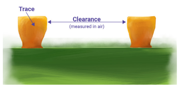
The standard outlines clearance requirements for common design elements, including component leads, uncoated conductive hardware, test probe sites, mounting hardware, and plated through-hole (PTH) reliefs in heat sinks. These values account for electrical safety, mechanical tolerances, and manufacturing variations. See the table below for details:
| Feature | Clearance |
|---|---|
| Component leads | 0.13 mm (up to a voltage of 50V) |
| Uncoated conducting areas (washers or similar mechanical hardware) | 0.75 mm |
| Test probe sites | 80% of the component height (0.6 mm minimum and 5 mm maximum) |
| Mounting hardware | Should not protrude more than 6.4 mm below the PCB surface |
| PTH relief in the heat sink | 2.5 mm larger than the hole (includes electrical clearance and misregistration tolerance) |
IPC-2221 also defines solder mask–related spacing to prevent bridging and ensure manufacturability.
| Mask type | Clearance | Dam |
|---|---|---|
| Liquid screenable | 0.25 mm | 0.25 mm |
| Photoimageable dry film ≤0.0635 mm | 0.051 mm | 0.127 mm |
| Photoimageable dry film 0.066 to 0.1 mm | 0.051 mm | 0.25 mm |
| LPI | 0.051 mm | 0.1 mm |
To learn about prevalent solder mask errors and techniques to avoid them, see 6 common solder mask errors every PCB designer should know.
What is creepage in PCB design?
Creepage describes the distance between conductors measured along the surface of an insulating material. IPC-2221 emphasizes maximizing this distance wherever possible to reduce the risk of surface leakage, especially in contaminated or high-humidity environments.
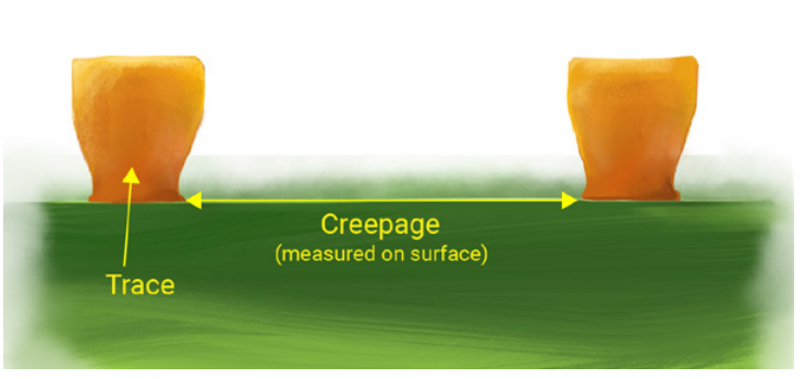
To achieve reliable creepage spacing, conductor separation must account for etch compensation, conductor edge imperfections, and copper wicking effects between plated through-holes and adjacent plane layers. The standard recommends allocating space equal to twice the etched copper thickness for compensation, ensuring that electrical clearance is maintained after fabrication.
How to determine PCB trace width?
PCB trace width is calculated based on the operating current, allowable temperature rise, and board construction constraints. These parameters work together to define the copper cross-section needed to prevent overheating and ensure long-term reliability.
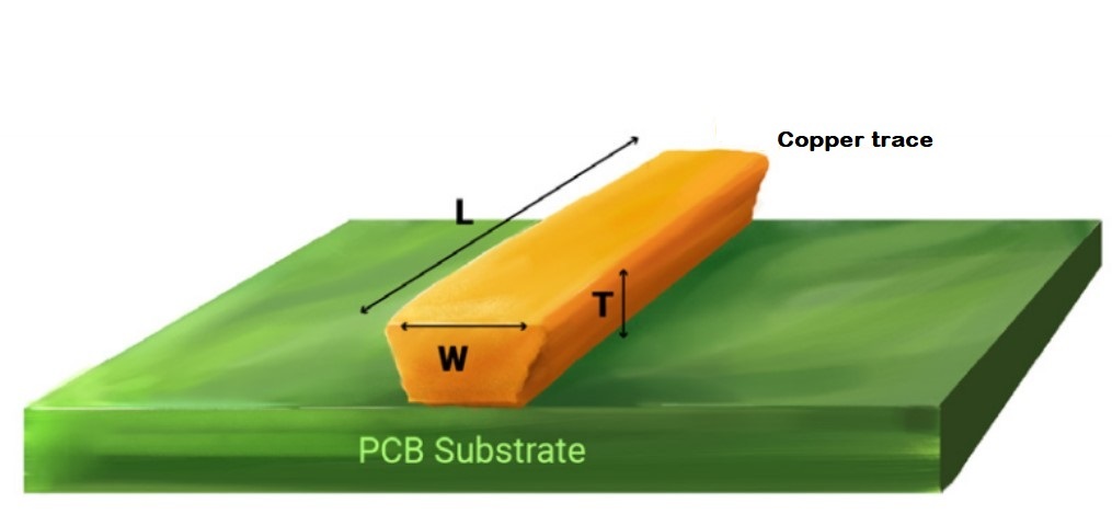
To calculate the trace width for allowable current, the following formula can be used:
Width [mil]=Area [mil2] / (Thickness [oz] x 1.378 [mil/oz])
The cross-sectional area, A is calculated by:
A = ( I / [k x (ΔT0.44)](1/0.725)
Where I is the maximum current in Amps, k is a constant, ΔT is the temperature rise above ambient in °C, and A is the cross-sectional area of trace in mil².
For internal layers,
- k = 0.024
- Conductor thickness = copper foil thickness of the base laminate.
- If blind and buried vias are implemented, then, the conductor thickness includes the copper plating thickness as well.
For external layers,
- k = 0.048
- Conductor thickness = thickness of the base foil and the plated copper of PTH without including the thickness of the solder coating, tin-lead plating, or secondary plating.
Trace dimensions are controlled by electrical, thermal, and manufacturing considerations. The effective copper cross-section depends on trace width, copper thickness, signal characteristics, and heat dissipation conditions.
Initial guidance for conductor sizing can be obtained from IPC-2221, while IPC-2152 (which supersedes the previous standard IPC 2221) provides empirically derived data for accurately determining trace width based on current and temperature rise. Board construction further influences these decisions; designs involving sequential lamination, blind vias, or buried vias require careful selection of copper thickness on individual layers.

What insulation resistance tests does IPC-2221 recommend?
IPC-2221 proposes insulation resistance tests and HiPot tests to assess PCB dielectric strength against voltage-induced leakage or failure. These evaluations ensure material and process suitability for reliable performance in operational environments.
Let’s see how these tests work:
- Insulation resistance test: In this test, a voltage is applied across the circuit board, which induces current flow. This current is measured to calculate the quantifiable resistance value for the entire product’s insulation.
- HiPot testing: This kind of test is used to check whether the insulation provided is enough to protect the circuit board or not. For this test, a high voltage is applied to the board, and the resulting current flow through the insulation is measured. This current is called the leakage current, and it is measured using the HiPot tester. If the high voltage does not break down the insulation, then the insulation will be good enough to protect the board. This test is also known as the dielectric withstanding voltage (DWV) test and is usually carried out after the dielectric breakdown test.
What insulation resistance test coupons does IPC-2221 define?
IPC-2221 defines standardized test coupons to evaluate both bulk insulation resistance and surface insulation resistance under controlled electrical and environmental conditions. These coupons help assess the impact of moisture, material quality, cleanliness, and manufacturing residues on insulation reliability.
1. Insulation resistance test coupons
- Moisture and insulation resistance coupons: These test coupons help to evaluate the insulation resistance and the bulk resistance of the circuit board. Here, the board is inspected by exposing it to different humidity and temperature environments with specific voltages applied to it.
- E-coupon: The moisture and insulation resistance of the laminated base materials are verified using this coupon. A design with a maximum of 10 layers can be tested using an E-coupon.
- Legacy E coupon: This coupon with a Y pattern aids in evaluating the cleanliness and insulation resistance properties.
2. Surface insulation resistance coupons
The surface insulation resistance test coupons include the following:
- H coupon: This involves measuring the effects of the process or residues on the surface insulation resistance.
- Legacy H coupon: Higher-level insulation testing requires using the legacy H coupon, such as for PCBs used in telecommunications.
To learn the ways to manage black pads in ENIG surface finish, see how to work around black pads in ENIG finish.
Design considerations for high-voltage PCB layout
When designing high-voltage boards, you must select high-CTI insulation materials, increase clearance and creepage beyond standard IPC-2221 minimums, and implement physical isolation barriers to prevent flashover or arcing.
Let’s look into these in detail:
Select suitable insulation materials
The materials used for insulation play a prominent role in withstanding the high potential between two conducting features. The best way to guarantee good insulation in high-voltage circuits is by choosing materials with comparative tracking index (CTI) ratings that can withstand high voltages. CTI is the measure of the electrical insulation of a material by subjecting it to a high voltage and monitoring the voltage at which it breaks down.
Increase the clearance and creepage
With the increase in voltages, it is obvious that the clearance and creepage distance between traces and conducting features on the PCB should be increased. But we are working on circuit boards here, and hence, there is a limit to how these distances can be increased. The minimum creepage and clearances defined by the IPC-2221 will not be enough to prevent a flashover in this case. Therefore, different methods should be adapted to increase the clearance and creepage distances for a high-voltage design. They include:
- Create slots, v-grooves, or parallel-sided notches between the conducting features
- Incorporate SMT components in abundance on the board; the ones that require maximum clearance from each other can be placed on opposite sides of the board
- Install vertical insulator barriers in the space
- Place high-voltage circuits on the top side of the board and low-voltage ones on the bottom to mitigate the chances of flash-over or arcing
IPC-2221 is a reference document that lays down a number of design standards while designing a PCB. Adhering to these standards is crucial to realizing DFM, DFA, and DFT specs. Let us know in the comments section if you require any assistance to make your board manufacturable in the first go. Our design and manufacturing experts will be happy to help you.
Need guidance on which IPC standard to follow? Post your queries on SierraConnect. Our PCB experts will answer them.

About Poulomi Ghosh : Poulomi is a microwave engineer specializing in EMI, EMC, RF, and high-speed electronics. As a senior technical writer at Sierra Circuits, she creates advanced engineering articles and webinars for hardware engineers and PCB designers.


