


Contents

On-demand webinar
How Good is My Shield? An Introduction to Transfer Impedance and Shielding Effectiveness
by Karen Burnham
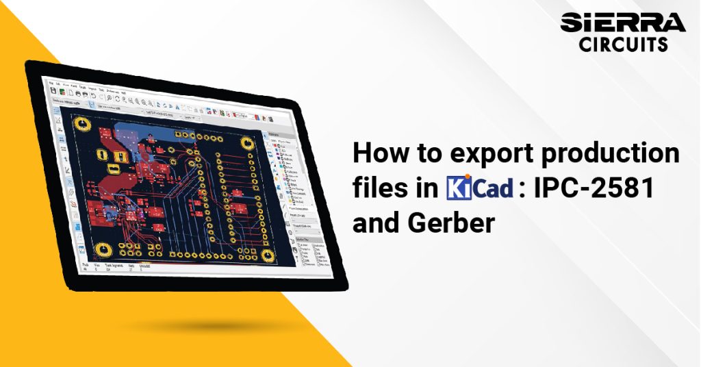
Exporting the correct design files is crucial for the smooth production of your PCB. KiCad supports industry-standard formats like IPC-2581 and Gerber. Each of these formats provides detailed information essential for different stages of production.
In this KiCad tutorial, you will learn how to export IPC-2581, Gerber, and other production files.
Production files supported by KiCad
After completing the design, the next step is to export production files in KiCad.
The set of files that are required for the production of PCBs is as mentioned below:
- IPC-2581: It is a unified design data format, enabling seamless data exchange between designers and fab houses.
- Gerber files: Gerber is a standard file format for exporting PCB designs. Your design will be saved and shared in this format for production.
These are the files containing production information for each layer of a PCB.
-
- Top etch
- Bottom etch
- Middle layer etch
- Top and bottom silkscreen
- Top and bottom paste mask
- Top and bottom solder mask
- Top and bottom assembly
- Fab details
- Board outline
- NC drill: This file gives information about all the holes required in the board. It will serve as an input to the drill machine to drill the required holes on the board.
- Component placement file: The machine uses this file to identify the X-Y location of the various components on the board using coordinates.
- IPC 356 netlist: It gives information about the connections between various components. Once you create your netlist, ensure it matches your schematic netlist.
- PDF: Generate PDFs for the following:
- Top and bottom assembly
- Fab details
- All layers
- Top and bottom silkscreen
- Board outline
- Schematic
- Stack-up report
- Top and bottom solder mask (optional)
- Top and bottom paste mask (optional)
- Bill of materials: The BOM consists of all the components used in your board and the manufacturer part numbers that will help the PCB manufacturer identify the components.
You need to export these production files using KiCad to manufacture your design. Let’s check how these files are generated in KiCad.
Steps to export production files in KiCad
Exporting the IPC-2581 file in KiCad
Step 1: Go to File –> Fabrication Outputs –> IPC2581 File (.xml). The Export IPC-2581 dialogue box will appear.

Step 2: Choose the destination folder and enter the output file name.

Step 3: Choose the desired measurement units, precision, and IPC-2581 version.

Step 4: Click Export to get started with the IPC-2581 file generation.

The unified file is then shared with the fabricators. They import the smart design data file using CAM systems to produce PCBs based on the design data provided by designers.
By using IPC-2581, you eliminate the need to generate separate files for Gerber, drill, and netlist, streamlining the design and manufacturing processes.
For step-by-step guidelines on designing a PCB using KiCad, download our eBook.

KiCad Design Guide
10 Chapters - 161 Pages - 180 Minute ReadWhat's Inside:
- Creating a component symbol library
- Setting up board parameters and rules
- How to route differential pairs
- How to place of components
Download Now
Exporting Gerber files in KiCad
Generating Gerber files in KiCad is a straightforward process. Follow these steps to export your PCB design for manufacturing.
Step 1: Click on Plot in the top toolbar.
Alternatively, you can go to File –> Plot from the menu bar.

This will open the Plot dialogue window, where you can configure the Gerber file settings.
Step 2: Configure the Gerber settings.

In the Plot dialogue window, choose the following settings:
- Choose Gerber as the output format from the Plot format dropdown menu.
- Specify the directory where you want to save the Gerber files. It’s a good idea to create a separate folder named “Gerber” within your project files to keep everything organized.
- Under the Include Layers section, select all the layers you need for the Gerber files. For a 4-layer PCB, select all four layers. Additionally, select:
- F.Paste (front paste)
- B.Paste (bottom paste)
- F.Silkscreen (front silkscreen)
- B.Silkscreen (bottom silkscreen)
- F.Mask (front soldermask)
- B.Mask (bottom soldermask)
- Edge.Cuts (defines the actual boundary of the PCB)
- F.Fab (front fab)
- B.Fab (bottom fab)
- Select the Edge.Cuts and User.Drawings layers options under Plot on All Layers. This will ensure the board outline and fabrication details are visible on all layers.
- Under General Options, make the following selections:
- Deselect Plot footprint values as component values are typically not plotted on the PCB.
- Check Plot reference designators, Plot footprint text, Sketch pads on fabrication layers, and Use drill/place file origin.
- Select Tent vias to cover vias with soldermask.
- Enable Subtract soldermask from silkscreen under Gerber Options to automatically remove any overlapping silkscreen from solder mask openings. While fab houses usually handle this, you can also configure it in KiCad.
- Check Use extended X2 format if supported by your fabrication house. If your manufacturer doesn’t support X2, uncheck the option to use the standard format.
Step 3: Once all settings are configured, click Plot to generate the Gerber files. The files will be saved in the directory you specified.
After the files are generated, check the Output Messages section in the Plot dialog to confirm that all files were successfully created.

Keep the dialog open for any additional steps, such as generating drill files or making final adjustments.
Your Gerber files are now stored in the designated folder, ready to be sent to your manufacturer.
Check the generated files for common problems associated with Gerber files, such as incomplete files, empty Gerber files, unregistered layers, etc.
Checklist for generating Gerber files
Once the routing is completed, you can export the Gerber files. However, ensure your design accurately matches the schematics and layout before generating them.
To ensure that, we have created a checklist below.
1. Bill of materials (BOM)
Ensure that the PCB bill of materials accurately reflects the schematic, confirming that component footprints, values, and other details match the manufacturer’s part numbers.
2. Schematic
Verify that all component values are correct, components are placed properly, and quality markings are accurate within the circuit.
3. Layout
Check whether you have placed all components required for manufacturing as per your design requirements.
Include any necessary details in the fabrication drawing, such as fab, dimensions, and stack-up data.
Generating drill files
Step 1: After generating the Gerber files, in the Plot dialog box click on Generate Drill Files.

A new Generate Drill Files window will appear.
Step 2: Configure the settings in the Generate Drill Files window.

- Select the Output folder where you want to save the file. Save the drill file in a separate drill folder.
- Make sure you have selected PTH and NPTH in single file.
- Choose Gerber X2 as the drill file format only if your fab house supports it.
- Select the Dill origin as Drill/place file origin.
- Select the Drill units as Inches.
- Under Map File Format, choose PostScript.
Step 3: Click Generate Drill File to create the drill file.
Step 4: To create a map file that shows the dimensions of the holes in the drill chart, click on Generate Map File. Select Gerber X2 as the preferable map file format before generating the file.

Step 5: Save the map file in the same location as your Gerber files. After saving, you will receive a notification in the Messages box confirming that the files have been saved.
Need help exporting Gerber and production files from KiCad? Our engineering team can assist you with Gerber generation, layer stack-up documentation, and fabrication-ready outputs for seamless manufacturing.
You can book a meeting with our experts or call us at +1 (800) 763-7503.

Saving the component placement files
Step 1: Go to File > Fabrication Outputs > Component Placement (.pos, .gbr).

Step 2: The Generate Placement Files window will appear. Choose the settings to generate the position file.

- Select the Output directory where you want to save the file.
- Under Format, select CSV, which will generate the position file in an Excel format.
- Select the Units in Inches.
- Under Files, if you select Single file for board, all the top and bottom components will be in a single file. To generate two different files for the top and bottom layers, select Separate files for the front, back.
Step 3: Click the Generate Position File to create the component placement file.

This saves the placement file in an Excel format in the selected folder.
After the file is saved, you will receive a notification about the saved file location in the Output Messages box.

The placement file in KiCad provides the precise X-Y coordinates for each component on the PCB, allowing the assembly machine to accurately place components in their correct positions on the board during manufacturing.
KiCad version 9 introduces enhanced STEP export functionality, allowing you to export a selected subset of components directly from the PCB editor.
Downloading the netlist file from the PCB layout editor
Step 1: Go to File > Fabrication Outputs > IPC-D-356 Netlist File.

Step 2: Choose the location to save the file. Enter the file name and save it. The netlist file will be exported to this location.

Exporting BOM file
Step 1: Go to File –> Fabrication Outputs —> Bill of materials.

Here, we need to follow the steps similar to the ones we used for netlist generation.

Generating PDFs
Follow these steps to generate PDFs in KiCad.
Step 1: Click on the Plot in the top toolbar.
Step 2: In the Plot window, under Plot format, select PDF.

Step 3: Configure the following settings to generate a PDF.

- Select the Output directory where you want to save the file.
- Under Include Layers, select F.Fab (front fab) and B.Fab (bottom fab).
- Under Plot on All Layers, select Edge.Cuts.
- In General Options, select:
- Plot footprint values
- Plot reference designators
- Plot footprint text
- Force plotting of invisible values/refs
- Sketch pads on fabrication layers
- In General Options, deselect Check zone fills before plotting.
- Deselect Use drill/place file origin.
After selecting the desired options, click on Save.
Step 4: Click on Plot to generate the top and bottom PDF files.
The top section will include your assembly information, showing the placement of your components.

The bottom of the PDF will display all the outlines and various designators.

Generating a PDF of fabrication details in KiCad
Step 1: Open the Plot dialog by clicking on Plot from the toolbar.
Step 2: Configure the settings for the PDF output. Under Plot format, select PDF from the dropdown. Under the Output directory, choose where you want to save the PDF.
Step 3: In the Plot window, under the Include Layers section, select User.Drawings. Uncheck all the other layer options.
Under Plot on All Layers, select Edge. Cuts. Retain all the other settings in the Plot window.

Step 5: Click Plot to generate the PDF for the User.Drawings layer. This PDF will contain all relevant fabrication details, including the board outline, dimensions, characteristics, and stack-up information.

Download our eBook for step-by-step guidance on creating custom libraries and linking symbols to footprints in KiCad 9.

KiCad 9 Step-by-Step Guide
6 Chapters - 41 Pages - 30 Minute ReadWhat's Inside:
- A complete KiCad 9 workflow from project creation to production file generation
- Step-by-step guidance on creating custom libraries and linking symbols to footprints
- Practical design checks: ERC and DRC
- Best practices for generating a clean BOM and fabrication-ready Gerber files
Download Now
Verifying production files using Gerber Viewer in KiCad
Gerber Viewer is a powerful tool that allows you to view and verify Gerber files, which are used to describe the layers of a printed circuit board.
Step 1: Click on the Gerber Viewer in the KiCad project manager window with various tools listed.

Step 2: To load Gerber files into Gerber Viewer, click on File –> Open Gerber Plot Files(s).

Select all the Gerber files and hit Open.

You can load multiple Gerber files at once, each representing different layers of your PCB (e.g., top copper, bottom copper, solder mask, etc.).
Step 3: To load drill files (usually with extensions like .drl) in Gerber Viewer, click File > Open Excellon Drill File(s).

Then browse and select your drill file from the location where it was saved and click Open.
Step 4: To view and verify the drill map, click on its layer file in the Layer Manager.

The drill map file typically has a .gpr extension. It contains detailed information about all the drill holes in your PCB, including the quantity of each hole size (e.g., 4 holes, 12 holes, 28 holes), their sizes in millimeters and inches, and the shapes assigned to each hole.
To ensure everything matches the drill map, click on both layers (drill file and drill map) in the Layer Manager. Cross-check that all the drills are correctly aligned and overlapped.

Step 5: View and analyze the Gerber Files on the right side of the Gerber Viewer window. You’ll see a list of loaded layers.
You can select each layer from the Gerber Viewer by checking or unchecking the boxes next to the layer names to check whether all the files in the board follow the layout design. You can also select several layers at a time for an overlapping view.

Once your files are verified, you can send the files for manufacturing. Send the files in a single zipped compressed file format. This will ensure that there are no errors during the transmission of the files.
You need to check and verify each of your layers and the edge cuts carefully. If you find errors in Gerber Viewer, you’ll need to go back, fix the errors in your layout, and then re-generate Gerber files using the plot tool. It is easier to fix them at this point as it won’t be easy later on.
If you want to validate the KiCad design files and get a real-time cost estimate, check out our KiCad Quote Plugin. This will enable you to get an instant quote without quitting the KiCad user interface.
Have queries on PCB design, assembly, and manufacturing? Post them on our forum, SierraConnect; our experts will resolve them.

About Pooja Mitra : Pooja Mitra is an electronics and communication engineer. With an experience of over three years in the PCB industry, she creates industry-focused articles that help electrical and PCB layout engineers.


