Speak to an Account Manager
![]() +1 (800) 763-7503
+1 (800) 763-7503
Tools for Designers:
Via Impedance Calculator
Try This New ToolSierra Circuits’ Via Impedance Calculator uses the physical dimensions of a via to calculate its capacitance, inductance, and impedance. The tool implements numerical solutions of Maxwell’s equations to render accurate and consistent results.
Vias (plated holes) are used to route electrical signals among different layers of a multilayer layer PCB. These holes comprise barrels, pads, and annular rings. The physical dimensions of these attributes affect the impedance, capacitance, and inductance of a via. Via design is also affected by the presence of a second ground plane and the distance between the ground planes. Thus, it is crucial to know the precise values of these parameters during the design phase to maintain the signal integrity of your system.
Features of the Via Impedance Calculator
1. You can choose from two different via models (through-hole, and laser via models). Each of these models has four via structures. The below table lists all the via structures supported by this tool.
| Through hole models | Laser via models |
|---|---|
| Through hole via | Blind via |
| Through hole via with two reference planes | Blind via with two reference planes |
| Through hole back-drilled via | Buried via |
| Through hole back-drilled via with two reference planes | Buried via with two reference planes |
2. It calculates capacitance, inductance, characteristic impedance, propagation delay, propagation delay per unit length, and effective dielectric constant of the selected via model.
3. The units of the input parameters can be changed among mils, centimeters, millimeters, and inches.
How to use Via Impedance Calculator
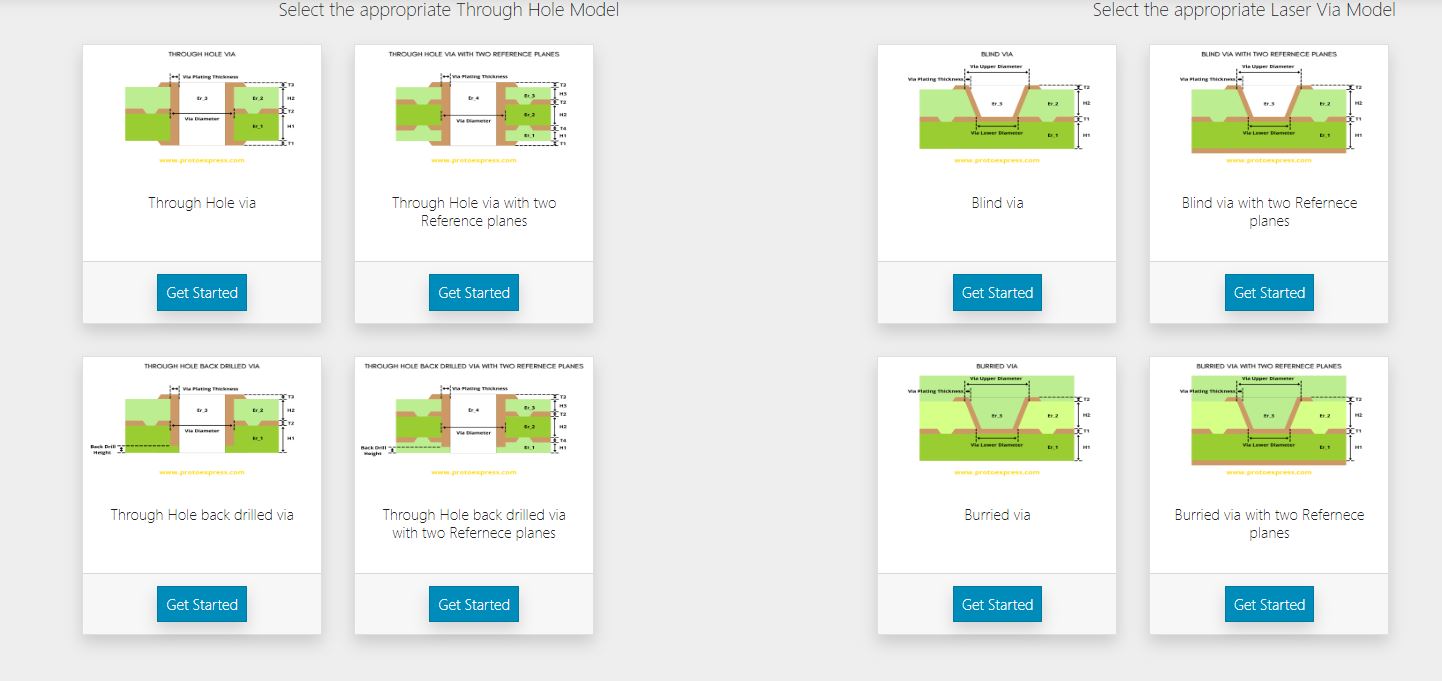
To begin, you need to select the appropriate via model. The available models are:
Through-hole models
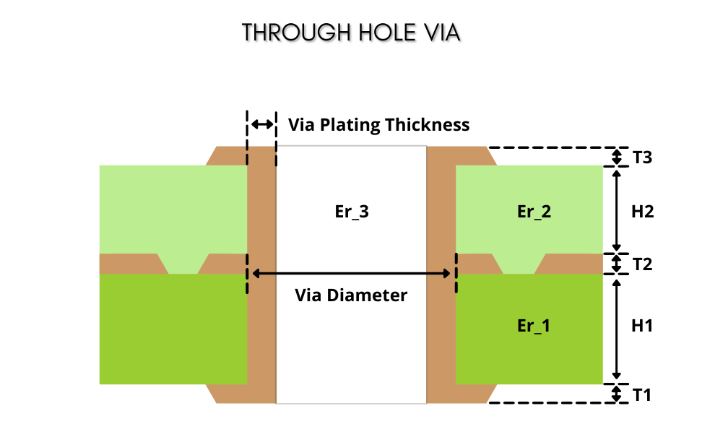
Through-hole vias pass through the entire board from the top layer to the bottom layer. Reference planes in a circuit board stack-up provide a return path for signals. Through hole via models with single and two reference planes are shown below.
Through hole via with single reference plane
Through hole via with two reference planes
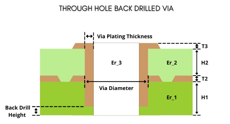
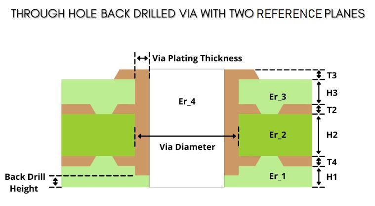
Through-hole back drilled vias
Back drilling involves drilling a hole slightly larger in diameter than the PTH to remove the conductive via stub. The structures of through hole back-drilled vias with single and two reference planes are shown below.
Through-hole back drilled via with single reference plane
Through-hole back drilled via with two reference planes
Laser via models
Laser vias are drilled using highly concentrated laser energy. The Via Impedance Calculator supports 4 different laser via structures. They are:
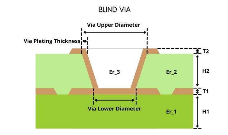
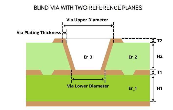
Blind via
Blind via is a hole that runs from an outer layer to the inner layer but not through the entire circuit board. The structures of blind via with single and two reference planes are shown below.
Blind via with single reference plane
Blind via with two reference planes
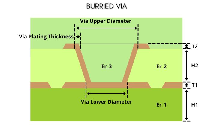
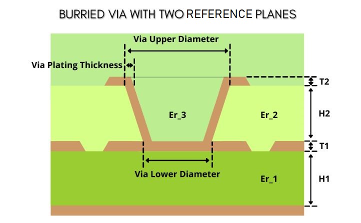
Buried via
Buried vias are located in the inner layers and have no paths to the outer layers. They connect the inner board layers and stay hidden from sight. The models of buried vias with single and two reference planes are shown below.
Buried via with single reference plane
Buried via with two reference planes
For now, let’s choose the through hole via with single reference plane.
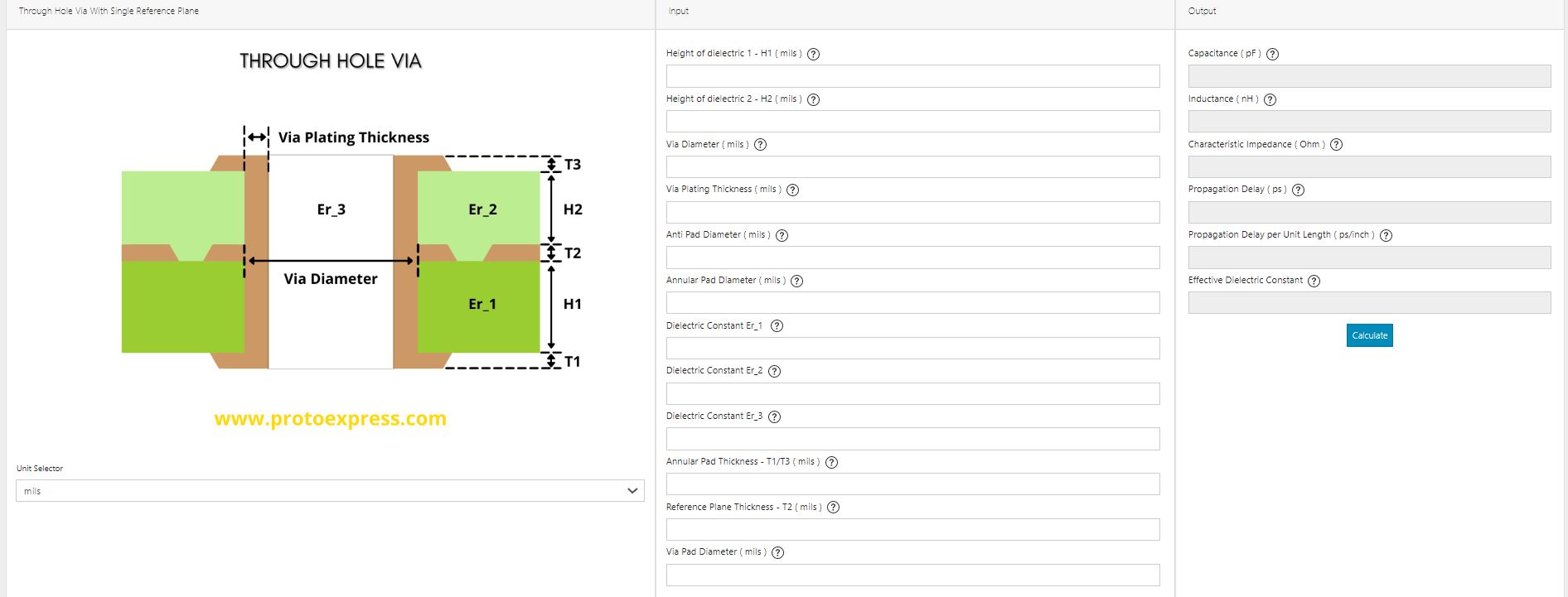
The input parameters for this model are:
- Height of dielectrics 1 and 2
- Via diameter
- Via plating thickness
- Anti pad diameter
- Annular pad diameter
- The dielectric constant of the dielectric below the reference plane
- The dielectric constant of the dielectric above the reference plane
- The dielectric constant of the dielectric on the inner surface of the via
- Annular pad thickness
- Reference plane thickness
- Via pad diameter
Please note that if you select any of the back-drilled via structures you will have to input the back drilled height along with the above-listed parameters.
After keying in all the input parameters, hit the calculate button present at the output section. The calculator will now display the values of the following output parameters:
- Capacitance
- Inductance
- Characteristic impedance
- Propagation delay
- Propagation delay per unit length
- Effective dielectric constant
If you’d like to know more about any of these input/output parameters, click on the help (?) button.
Controlling the impedance, capacitance, and inductance of a via is an essential prerequisite for ensuring signal integrity of your high-speed design. Sierra Circuits’ Via Impedance Calculator enables you to calculate optimum values of these parasitic elements based on the physical dimensions of a via.
Watch the tool demo:

Sierra Circuits has developed easy-to-use tools for PCB designers and electrical engineers at every stage of circuit board development.


Fabrication, Procurement, & Assembly. PCBs fully assembled in as fast as 5 days.
- Bundled together in an entirely-online process
- Reviewed and tested by Engineers
- DFA & DFM Checks on every order
- Shipped from Silicon Valley in as fast as 5 days

Fabrication. Procurement & Assembly optional. Flexible and transparent for advanced creators.
- Rigid PCBs, built to IPC-6012 Class 2 Specs
- 2 mil (0.002″) trace / space
- DFM Checks on every order
- 24-hour turn-times available

Complex technology, with a dedicated CAM Engineer. Stack-up assistance included.
- Complex PCB requirements
- Mil-Spec & Class 3 with HDI Features
- Blind & Buried Vias
- Flex & Rigid-Flex boards