What is characteristic impedance?
Characteristic impedance or surge impedance is the impedance of a PCB transmission line without including the effect of other transmission lines. It is the ratio of voltage and current amplitudes of a single wave propagating along the line in the absence of reflections from other directions. The characteristic impedance is generally defined to be 50 ohms and may take a different value based on the signaling standard used.
A cable that connects an antenna to a TV is a simple example of controlled impedance. It is important to maintain the dimensions of the cable conductors, shield, and insulator along with the electrical characteristics of the insulator to determine the interaction of the electrical fields, thus impedance of the cable.
In the same way, several trace configurations are used in a circuit board design to achieve controlled impedance. Boards with controlled impedance imitate the CI cables. To elaborate, the coax shield represents the plane, the laminate represents the insulator, and the PCB trace signifies the conductor.
When a circuit board operates at a high frequency, its traces act like transmission lines. The impedance variations from one point to the following points cause reflection in these transmission lines. This reflection superimposes the primary signal by traveling in the opposite direction. It results in distortion in the primary signal. Accordingly, a faulty signal appears at the receiver input. Therefore to have an undistorted signal at the receiver, the board signal traces must have a uniform controlled impedance to minimize the reflections. This is the first step to improving the integrity of the signals on board. Standard tolerance for controlled impedance is +/-10% ohms. Sierra Circuits offers tighter tolerances of +/-5% ohms.
Uniform controlled impedance
Controlled impedance is the characteristic impedance of a transmission line formed by a trace and its associated reference planes. It is relevant to the AC behavior of high-frequency signals (above 100MHz) propagating through PCB transmission lines. A uniform controlled impedance is important to achieve good signal integrity, i.e., the propagation of signals without significant distortion.
Controlled impedance traces are determined by their physical dimensions and the property of the dielectric material used in the circuit board. The most common examples of transmission lines that require controlled impedance are single-ended microstrip, single-ended stripline, microstrip differential pair, and stripline differential pair. Maximum power can only be transferred through a trace when the impedances are matched. This is what we need to accomplish in our designs.
What is the difference between characteristic impedance and controlled impedance?
Characteristic impedance is evaluated considering a single transmission line. Whereas, controlled impedance is achieved by matching the PCB substrate material properties with trace dimensions and locations. Controlled impedance is implemented to ensure the signal trace impedance remains consistent and within the range.
Controlled impedance design checklist
- Identify which signals require controlled impedance: Always refer to the datasheet to identify the signals that require CI. Some of the examples of controlled impedance traces are DDR traces, Gigabit Ethernet traces, RF signals, etc. Identify the frequency at which the signals propagate.
- You should know the impedances of some standard interfaces: Check the table given below.
| Type of interface | Differential impedance | Single-ended impedance |
|
|---|---|---|---|
| 1. | PCI Express | 90Ω ±15% | 50Ω ±15% |
| 2. | SATA | 90Ω ±15% | 55Ω ±15% |
| 3. | Ethernet | 95Ω ±15% | 55Ω ±15% |
| 4. | USB 2.0 signals | 90Ω ±15% | 50Ω ±15% |
| 5. | USB 3.0 signals | 90Ω ±15% | 50Ω ±15% |
| 6. | Parallel RGB LCN | N/A | 50Ω ±15% |
| 7. | LVDS LCD | 100Ω ±15% | 55Ω ±15% |
| 8. | HDMI/DVI | 90Ω ±15% | 50Ω ±15% |
| 9. | Analogue VGA | N/A | 50Ω ±15% 75Ω ±15% |
| 10. | Parallel camera interface | N/A | 50Ω ±15% |
| 11. | SD/MMC/SDIO | N/A | 50Ω ±15% |
| 12. | I2C | N/A | 50Ω ±15% |
| 13. | Display serial interface (MIPI/DSI with D-PHY) | 90Ω ±15% | 50Ω ±15% |
| 14. | Camera serial interface (MIPI/CSI-2 with D-PHY) | 90Ω ±15% | 50Ω ±15% |
- Stack-up design: Decide on the number of layers and stack-up material.
- Calculate the trace parameters for controlled impedance: Determine trace thickness, height, and length along with the dielectric constant of the material. Inform the manufacturer about the number of layers, the value of impedance traces, and PCB material.

Controlled Impedance Design Guide
6 Chapters - 56 Pages - 60 Minute ReadWhat's Inside:
- Understanding why controlled impedance is necessary
- Stack-up design guidelines
- How to design for impedance
- Common mistakes to avoid
Download Now
Note: Special software and tools such as Instack and Sierra Circuits impedance calculator are used to compute the trace impedance.
- Specify controlled impedance layout design guidelines (if any) to be followed by the layout designer, either in the schematic or in a separate read me file.
- Differentiate controlled impedance traces from normal traces: It allows the PCB manufacturer to easily recognize the controlled impedance traces. Sometimes manufacturers change the trace width to achieve a certain impedance value.
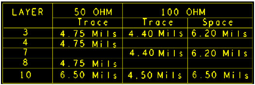
| Differential pair 90 Ω | Differential pair 100Ω |
||||
|---|---|---|---|---|---|
| Layer | 50Ω (SE) | 90Ω trace | 90Ω space | 100Ω trace | 100Ω space |
| 1 | 4.3 mils | 4.25 mils | 6.25 mils | 3.5 mils | 7 mils |
| 3 | 4.2 mils | 4.4 mils | 6.1 mils | 3.6 mils | 6.9 mils |
| 6 | 4.2 mils | 4.4 mils | 6.1 mils | 3.6 mils | 6.9 mils |
| 8 | 4.3 mils | 4.25 mils | 6.25 mils | 3.5 mils | 7 mils |
- Route differential pair signal traces parallelly with a constant spacing between them to achieve symmetry.
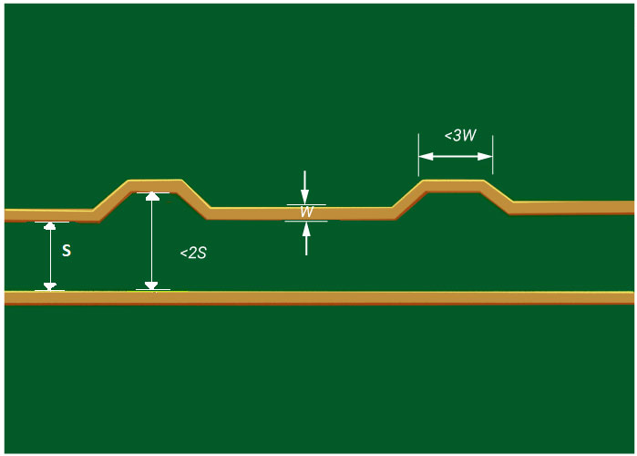
- Follow 3W and 2W rules to maintain adequate spacing between controlled impedance traces, other traces, and components.
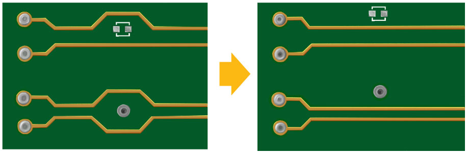
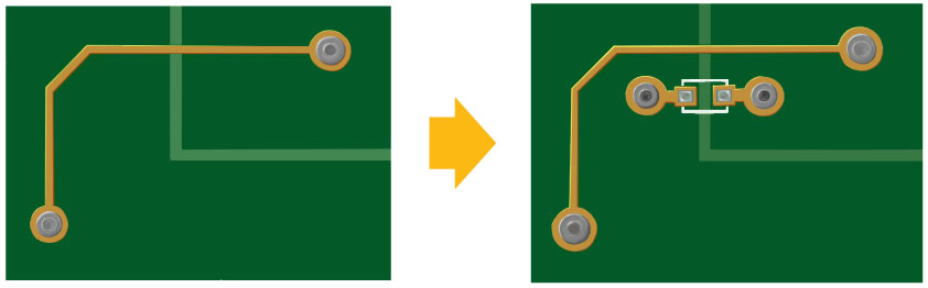
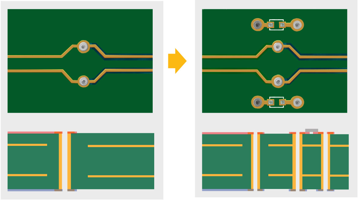
- Do not place components and vias between differential pairs: This practice removes the chances of impedance discontinuities caused due to vias.
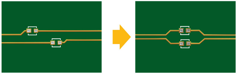
- Place serial coupling capacitors symmetrically when using high-speed differential pairs.
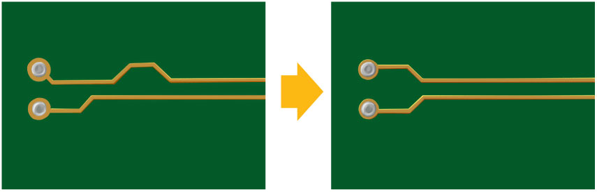
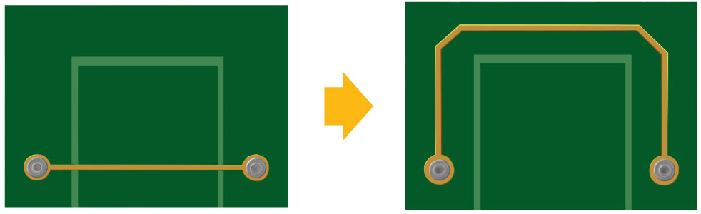
- Refrain from routing high-speed signals at plane and PCB borders.
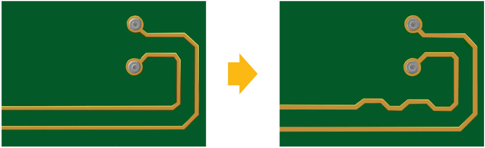
- Match the length of the traces forming differential pairs closely: It can be achieved by adding serpentines to the shorter trace.

Length matching for differential pairs - Place serpentine traces as near as possible to the source of mismatch.
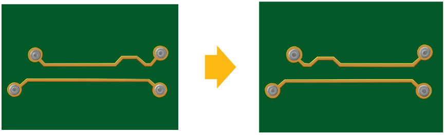
- Place serpentine traces as close as possible to the bend area.
- Provide reference planes nearest to the signal layer to achieve a continuous reference plane for signal return path.
- When routing signals over two different reference planes use a stitching capacitor.
- Add stitching capacitors when using power planes as reference.
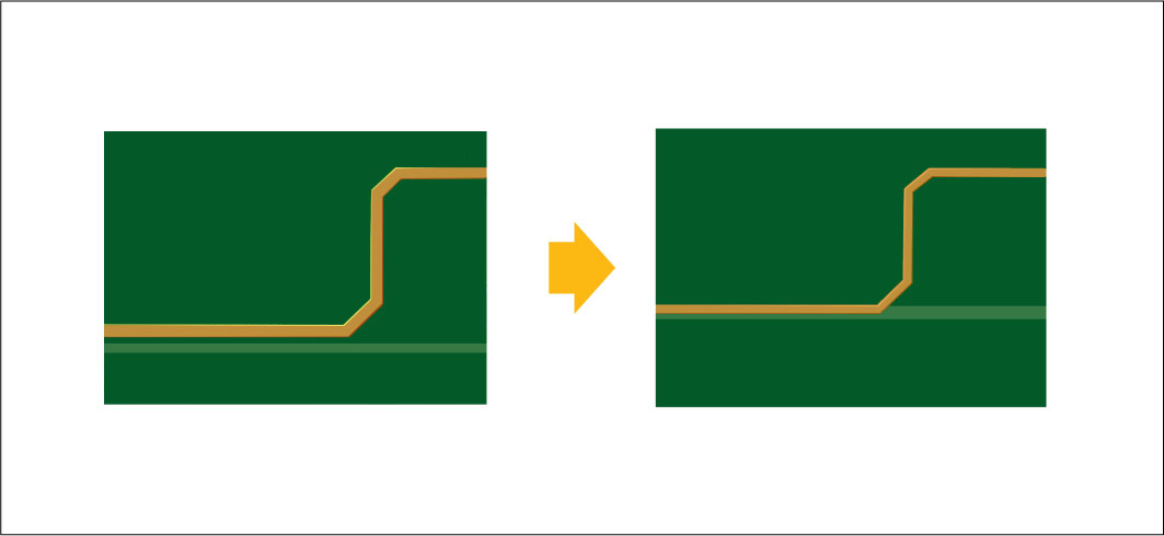
- When a differential pair or single-ended signal switches layers, add stitching vias close to the layer change vias.
- When changing the signal reference plane, add a stitching capacitor.
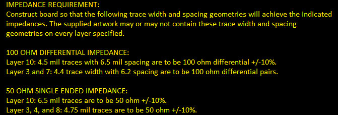
Fabrication drawing for controlled impedance
Fabrication notes, tables, and drawings contain necessary information such as impedance value, spacing, and layers.
A layout designer must include the impedance information in the fabrication drawing notes and tables. The information should include the impedance value, the trace width, the spacing for differential pairs, and the layer on which the controlled impedance traces are routed. Preferably, an impedance table should be part of the fabrication drawing.
PCB manufacturers will review these notes and create a stack-up to get the desired trace width and spacing.
They can make minor adjustments in the trace width and spacing to achieve the required impedance.
Key points to remember
Along with the usual PCB specifications, a designer should also specify:
- Which layers contain controlled impedance traces?
- The impedances of the traces since there can be more than one value of impedance trace per layer.
- Separate aperture codes for controlled impedance traces, e.g., 4 mil non-controlled impedance trace and 4 mil-controlled impedance trace.
- Matched impedance between the driver and the load is the key to achieving distortionless signal transmission.


