Vias in PCBs are a means of establishing interconnections between different layers. We know that vias are plated with copper for conductivity. But if the remaining part of the via opening is left as it is, without covering, then there are chances of solder paste seeping inside them. This might eventually lead to a short circuit. There are also chances of dust particles and remnants of any mechanical process getting inside the via. To avoid all these, via covering is introduced. Via covering is commonly called via tenting.
What is via covering in circuit boards?
Via covering is usually a solder mask or any other non-conductive material that protects the via from the entry of solder paste, dust, or any other particles. Open vias are not preferred because they may cause accidental conductive paths due to accumulated solder paste. There are three types of via coverings: via tenting, via plugging, and via filling.
Why are via holes covered with solder mask?
As described earlier, a via hole is covered with solder mask to prevent the entry of solder paste into it. This process is called via tenting, and the vias are thereby referred to as tented vias. Via tenting is an economic process that requires very low cost and hence is more popular. This covering can be done on a blind vias or through-hole vias.
Generally, vias that come under components are tented as there is a high risk of solder paste seeping through the via to the other side of the board.
How via tenting is achieved in circuit boards
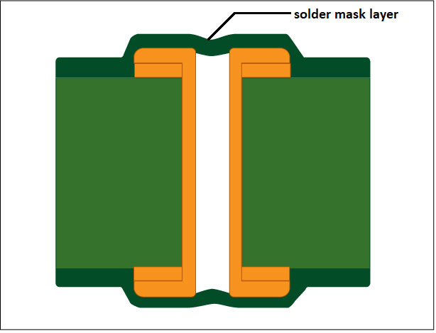
A liquid photo-imagable solder mask is used for tenting in PCBs. This film completely covers the via opening. Through-hole vias should be tented on both sides to reduce the chances of any chemical entrapment. If any gases are trapped inside the via, there are chances of them getting expanded later on during any other process. This may affect the reliability of the board.
Vias with one end tented and the other open can have residual etchants trapped in them during the etching process. These chemicals will crystalize and form copper sulfate crystals. These also affect the PCB’s reliability. Usually, via tenting is done on vias less than or equal to 0.3 mm (diameter).
To know more about via tenting design rules, read PCB via tenting design rules and fabrication notes.
What is via plugging in PCB?
Via plugging is another method of via covering where the vias are filled with a non-conductive material like epoxy. No other surface finish is applied to the via or its barrel. Plugged vias are fully filled. The material for filling can be applied on a single side or both sides. The vias considered for plugging should have a diameter between 0.4 to 0.5 mm.
Via tenting Vs. via plugging
| Via tenting | Via plugging |
|---|---|
| The top of the annular ring is covered to prevent the solder from seeping into the hole. | The vias are filled with non-conductive epoxy and cured. |
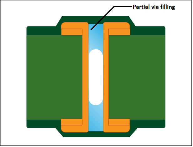
| The hole can be partially filled with an LPI solder mask or the filling can be washed off. | Plugged vias are fully filled. |
| Through-hole vias should be tented on both sides to reduce the chances of any chemical entrapment. | The material for filling can be applied on a single side or both sides. |
| Via tenting is done on vias with less than or equal to 0.3 mm diameter. | The vias considered for plugging should have a diameter between 0.4 mm and 0.5 mm. |
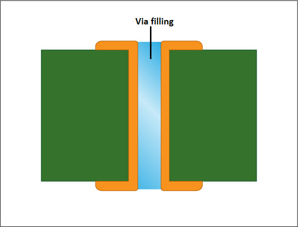
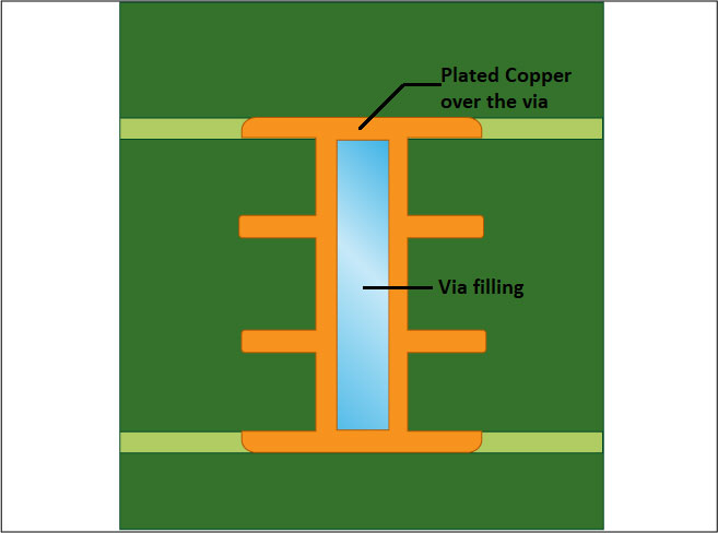
What is via filling?
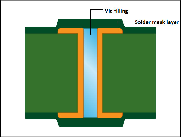
Via filling is the process of filling vias with a conductive or non-conductive medium. There may or may not be a solder mask layer after the filling. As per IPC-4761, filled vias can be of three types.
1. Filled vias: These are vias that are completely filled with a non-conductive/conductive filling.
2. Filled and covered vias: These vias are initially filled completely with a non-conductive/conductive medium and then covered with a solder mask layer.
3. Filled and capped vias: At first, a non-conductive/conductive medium is filled and is left for hardening. Next, the ends are planarized and metalized. Then these are plated over to make the surface solderable. This is the technology in via-in-pads. These types of vias help in saving space.
These are the basic types and classifications of via coverings on circuit boards. It is best to choose one of these depending on your budget, PCB design, and via properties required. To learn how to design vias, read how to design a via with current carrying capacity.

Signal Integrity eBook
6 Chapters - 53 Pages - 60 Minute ReadWhat's Inside:
- Impedance discontinuities
- Crosstalk
- Reflections, ringing, overshoot and undershoot
- Via stubs
Download Now


