


Contents
A PCB reflects every component footprint on it. This land pattern comes with a solder mask opening so that the components are soldered to their respective pads. This set of pads should be designed as per the IPC 7351 footprint standards for hassle-free board assembly.
What are the main features of IPC 7351?
As a designer, you aim to have a circuit board with signal integrity. To accomplish this, you need to follow industry standards in your board layout design, routing signals, and component placement. Whether it is a BGA, SMD, or through-hole component, the land pattern is essential for the PCB assembly process.
The IPC 7351 guidelines can help you achieve the best soldering quality while ensuring sufficient clearances for rework, testing, and inspection. Other important features of this document are:
- Provides the land pattern design specifications for active and passive components.
- Defines the courtyard dimensions, which are the minimum electrical and mechanical clearances of a component.
- Allows you to choose among the three land pattern topologies based on the component density of your design.
- Facilitates land pattern naming convention guidelines for components like resistor array packages, DFN devices, and flat lead devices.
In this section, you will learn the primary focal points defined by the IPC 7351 land pattern standard.
Check out our PCB component sourcing and stocking services to get your electronics to market fast!
3-tier library system for SMD components
Electronic products can be classified into three categories based on component density. They are level A, level B, and level C. The 3-tier CAD library system in IPC-7351 accommodates the various soldering standards and tolerances for each of these categories:
- Level A is defined for low-density component applications. This geometry is applicable to leadless chips and gullwing devices with leads. The specifications mentioned in this bracket can also be employed for inward and J-shaped lead contact devices.
- Level B applies to moderate-level component density products. It provides the median or nominal land pattern geometry. This standard defines the conditions for wave soldering of leadless chip and leaded gull-wing components.
- Level C provides the component footprint standards for high-density products such as mobile phones, medical devices, and other handheld applications.
To learn the new revisions of soldering benchmarks, see the new H revisions of IPC-J-STD-001 and IPC-A-610 soldering standards.
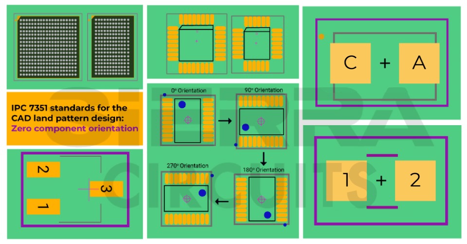
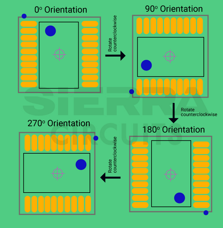
Zero component orientation
Zero component orientation enables manufacturers to standardize the orientation of the parts that come in various packaging methods, such as reels, trays, and tubes. This helps the pick-and-place machine to make the right decisions and place the components correctly. The table below defines the zero orientation locations for various components.
| Components | Zero orientation |
|---|---|
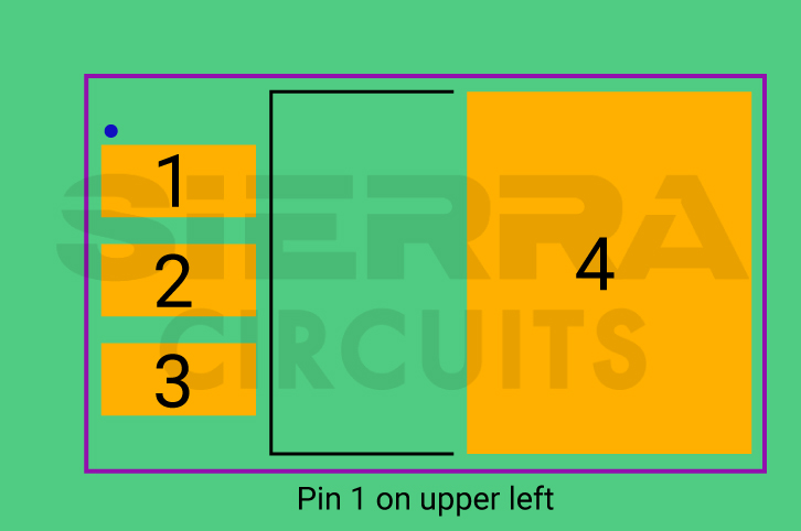
| Capacitors, resistors, and inductors | Pin 1 on left. It is always the positive pin |
| Diodes | Cathode on left. Pin 1 always marks the polarity of these devices |
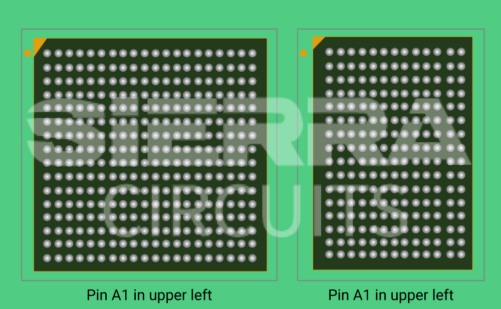
| SOT devices, ceramic flat packs, small outline J lead ICs, quad flat pack ICs, leadless chip carriers, and BGAs | Upper left |
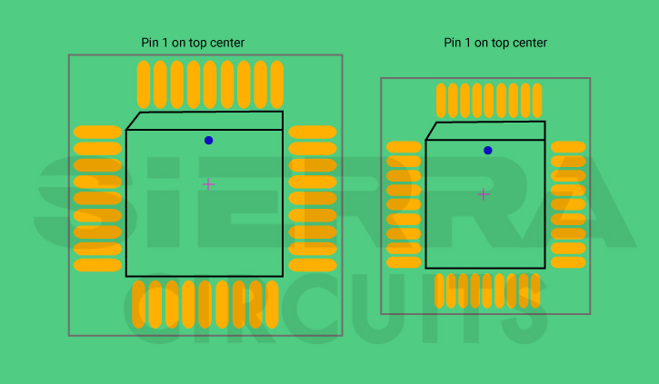
| Bumper and plastic quad flat pack ICs | Top center |
The image below illustrates the BGA pin orientation on the upper left.
Pin 1 orientation on the top left corner of a SOT component.
Pin 1 orientation on the top left corner of an IC.
The image below shows the placement of pin 1 for a chip capacitor.
It is very important to orient the pin as per the given guidelines so that when the component is rotated at any angle, the reference pin remains the same.
Read our case study on eliminating BOM and footprint errors in PCB assembly to learn how we worked with the designer to ensure accurate component orientation.

Land pattern naming convention
IPC-7351B provides the guidelines for the land pattern naming. Following these standards will help you standardize the schematic symbols:
- Express the lead span and height with two places after the decimal point and include trailing zeros.
- Place a “-” (dash) before the pin quantity.
- Use “_” (underscore) to separate the pin quantity of hidden and deleted components.
- Instead of using the term “by”, use the letter “X” to separate two integers, such as height X width.
A few examples of IPC 7351 land pattern naming conventions
| Component type | Footprint nomenclature |
|---|---|
| Chip capacitor | CAPCA + pitch P + body width X body length in metric - pin quantity |
| Chip inductors | INDC + body size in metric (body length + body width X height) |
| Molded LEDs | LEDM + body length + body width X height |
| Ceramic quad flat packages | 1.27 mm pitch : CQFP127P+ lead span L1 X lead span L2 nominal X height - pin quantity |
| Molded resistors | RESM + body length + body width X height |
| Small outline transistors (flat lead) | 1 mm pitch: SOP100P + lead span nominal X height - pin quantity |
| Ball grid array | 1.5 mm pitch: BGA150P +number of pin columns X number of pin rows-pin quantity |

Fill out the form:
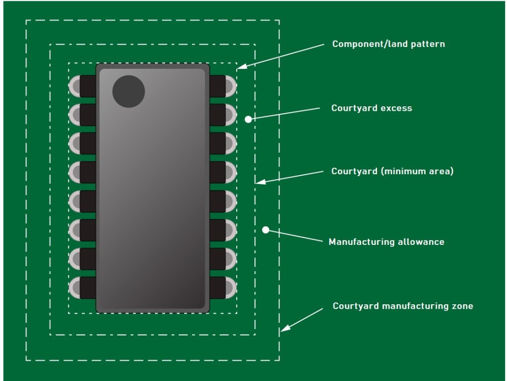
Standards for component placement courtyard
The courtyard is the rectangular area that defines the electrical and mechanical clearances around the component body. Courtyard excess is the area between the rectangle formed by the outer edge of the component footprint and the outer boundary of the courtyard.
To maintain sufficient spacing between the components and copper features, you need to ensure that placement courtyards do not overlap. IPC 7351 defines the standard courtyard parameters for different components.
Read how to place components in KiCad to learn the options available in the EDA tool for part placement.
Guidelines for silkscreen marking
Some of the significant guidelines for silkscreen markings present in IPC 7351 are:
- Never place the silkscreen outlines below the component, as they tend to get covered during the circuit board assembly.
- Place the silkscreen on the edge of the component that is used as crop marking.
- The polarity marking should highlight and indicate the pin 1 location. This should be visible even after the assembly process.
- The placement of all silkscreen outlines must be within the courtyard.
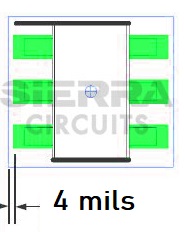
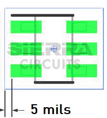
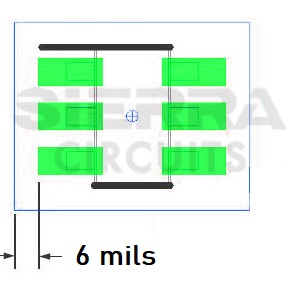
Silkscreen line width is the gap between the silkscreen and the land pattern. The images below depict the line width specifications that need to be maintained for different applications.
High component density: It is also called the least land protrusion environment and is employed for HDI PCBs. The recommended line width is 4 mil.
Median component density: This refers to the median land protrusion environment. It is preferred for moderate component density products. Provide the line width as 5 mil.
Low component density: This indicates that there is a maximum area for the land pattern. It can be used for low-density applications. The suggested line width as per IPC 7351 standards is 6 mil.

HDI PCB Design Guide
5 Chapters - 52 Pages - 60 Minute ReadWhat's Inside:
- Planning your stack-up and microvia structure
- Choosing the right materials
- Signal integrity and controlled impedance in HDI
- Manufacturing considerations for higher yields
Download Now
Land pattern layout for efficient component placement
The minimum space between the components is determined by factors like the surface area of the board, the type of device, and the operating speed.
Stick to the guidelines below for placing the components:
- Provide minimum spacing between the component packages to meet all the manufacturing requirements.
- Group similar components on the board. This will ensure proper component placement and facilitate efficient inspection and soldering processes.
- Isolate the analog and digital designs.
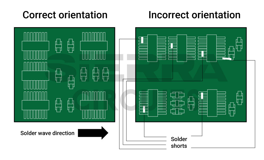
- Wave soldering is typically used to assemble through-hole components, while SMT components are soldered using reflow techniques. Therefore, place all the SMDs in the same direction as the solder wave. This will help you minimize the solder defects.
For more on efficient component placement, see component placement guidelines.
Difference between PCB land pattern and footprint
The terms land pattern and footprint are used interchangeably in the PCB manufacturing industry. However, there are certain differences between them when we consider their functionality. A component can have multiple land patterns based on the IPC density level (level A, level B, or level C according to IPC-7351), but there is always a single footprint.
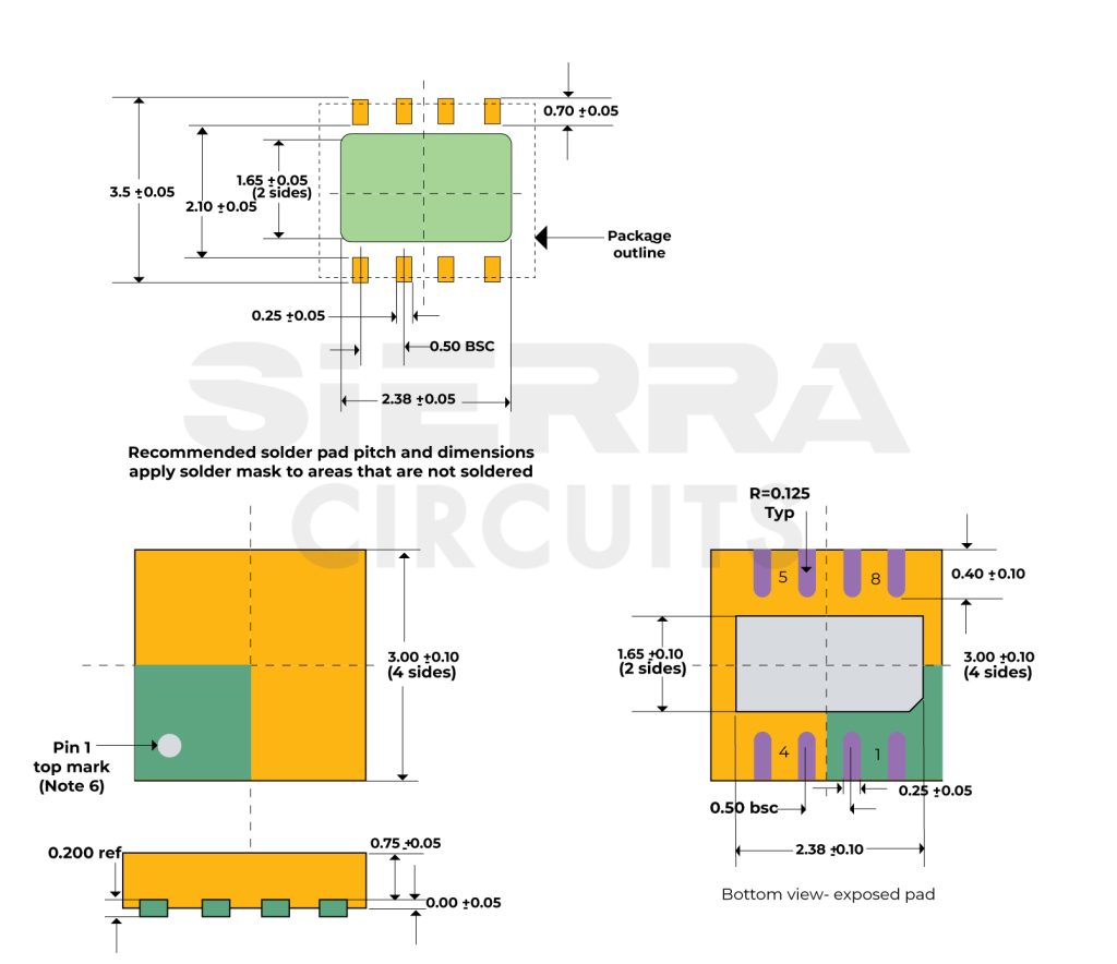
The land pattern in the datasheet provides details of pad sizes, the outline of the component, and tolerances. The pad dimensions will be slightly more than the leads to ensure an efficient electrical connection after the soldering process.
Additionally, it helps identify defects in the solder joint. Here’s an example of a component land pattern.
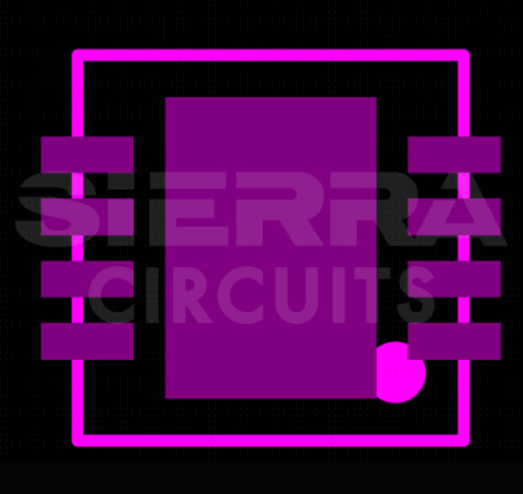
On the other hand, a PCB footprint gives an idea of the actual size of the component and provides information related to pad size, pin number, pitch, component outline, and the reference designator. For example, when we place a component on the sand, it will leave its impression there. This imprint is the actual physical size of the component. The footprint of a component includes:
- Component centroid
- Connector details
- 3D model step file
- Silkscreen information
- Mounting holes / SMT pads
- Component boundary
- Pin 1 marking
- Manufacturer part number
The image below shows the footprint of the component that was created using the land pattern shown in this section.

PCB Design for Assembly Handbook
6 Chapters - 50 Pages - 70 Minute ReadWhat's Inside:
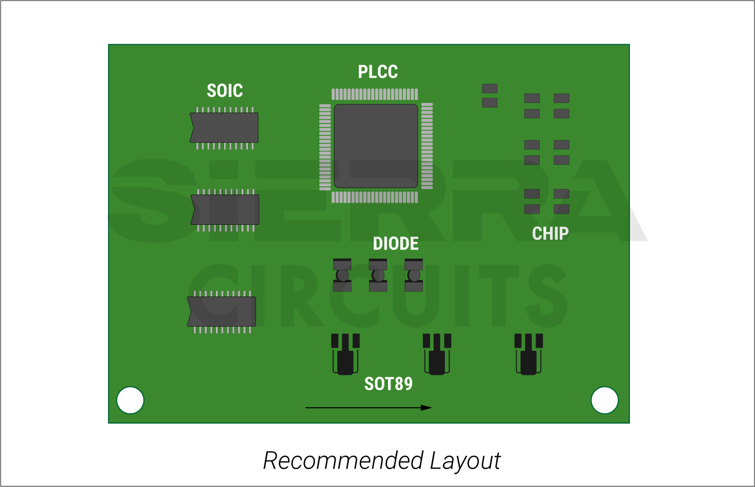
- Recommended layout for components
- Common PCB assembly defects
- Factors that impact the cost of the PCB assembly, including:
- Component packages
- Board assembly volumes
Download Now
Calculation of land pattern requirements for a small outline integrated circuits (SOIC) package
SOIC footprints vary depending on the package body size, pad spread, and lead pitch. It’s crucial to match the footprint dimensions with the tolerances of the package provided by the manufacturer.
IPC 7351 footprint standards define three equations to calculate the overall length (Zmax), the distance between pads(Gmin), and the width of the land pattern(Xmax):
Zmax = Lmin + 2Jt + sqrt(Cl²+F²+P²)
Gmin = Smax – 2Jh – sqrt(Cs²+F²+P²)
Xmax = Wmin + 2Js + sqrt(Cw²+F²+P²)
Where:
- Zmax = the overall length of the land pattern
- Gmin = the distance between the pads
- Xmax = the width of the land pattern
- Lmin = minimum length of the component (end to end)
- S = the distance between component terminations
- W = the width of the lead or termination
- Jt = the solder fillet or land protrusion at the toe
- Jh = the solder fillet or land protrusion at the heel
- Js = the solder fillet or land protrusion at the side
- Cl = the tolerance on component length
- Cw = lead width tolerance
- Cs = tolerance on the distance between component terminations
- F = fabrication tolerance
- P = placement tolerance
The IPC 7351 standard defines the size, shape, and tolerance for the surface-mount pads on your board. Adhering to these standards enables your manufacturer to establish a reliable electrical connection between the solder fillets and the components, avoiding manufacturing defects caused by land patterns.
Need help in designing reliable PCBs? Our engineering team can help you with thermal management, stack-up design, and DFM analysis.
You can book a meeting with our experts or call us at +1 (800) 763-7503.

In addition to this, it also ensures that the soldering process is as per the standard J-STD-001. A component’s land pattern will be generally available in your EDA tool library. However, if your design features a new component that is not listed in your tool library, you’ll have to manually design the footprint.
Need any assistance in creating a component land pattern for your design? Post your queries on our forum, SierraConnect. Our design experts will resolve them.

About Milan Yogendrappa : Milan Y is an electronics and communication engineer with over 6 years of experience in developing and editing technical articles related to PCB design, manufacturing, and assembly. He is currently the editor-in-chief at Sierra Circuits.


