Array panelization is implemented for high-volume board assembly. The whole panel is taken through the assembly lines and components are placed using automated machinery.
What is PCB panelization and why is it important?
PCB cores and laminations are typically available in sizes of 12 x 18 inches or 24 x 18 inches. Most of the time the circuits are much smaller than 12 x 18 inches. Therefore, this makes it possible to have multiples of the same circuit on a single panel. The number of circuits on the same panel will depend on the size of the board and the amount of space left for controlled impedance coupons. This process of fitting multiple circuits on the same panel is called panelization.
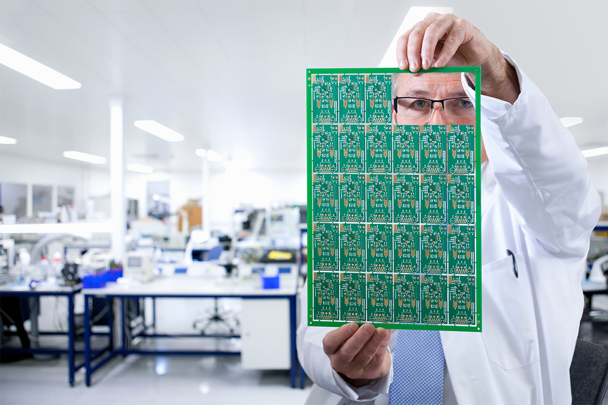
This large panel is then passed over the assembly line during the assembly process.
PCB panelization is important because it reduces the time and cost of the assembly process. A large panel is formed first and then individual smaller circuit boards are placed on it and processed further. In low-volume PCB manufacturing and assembly, panelization is not preferred.

PCB Design for Assembly Handbook
6 Chapters - 50 Pages - 70 Minute ReadWhat's Inside:
- Recommended layout for components
- Common PCB assembly defects
- Factors that impact the cost of the PCB assembly, including:
- Component packages
- Board assembly volumes
Download Now
How big is a board panel?
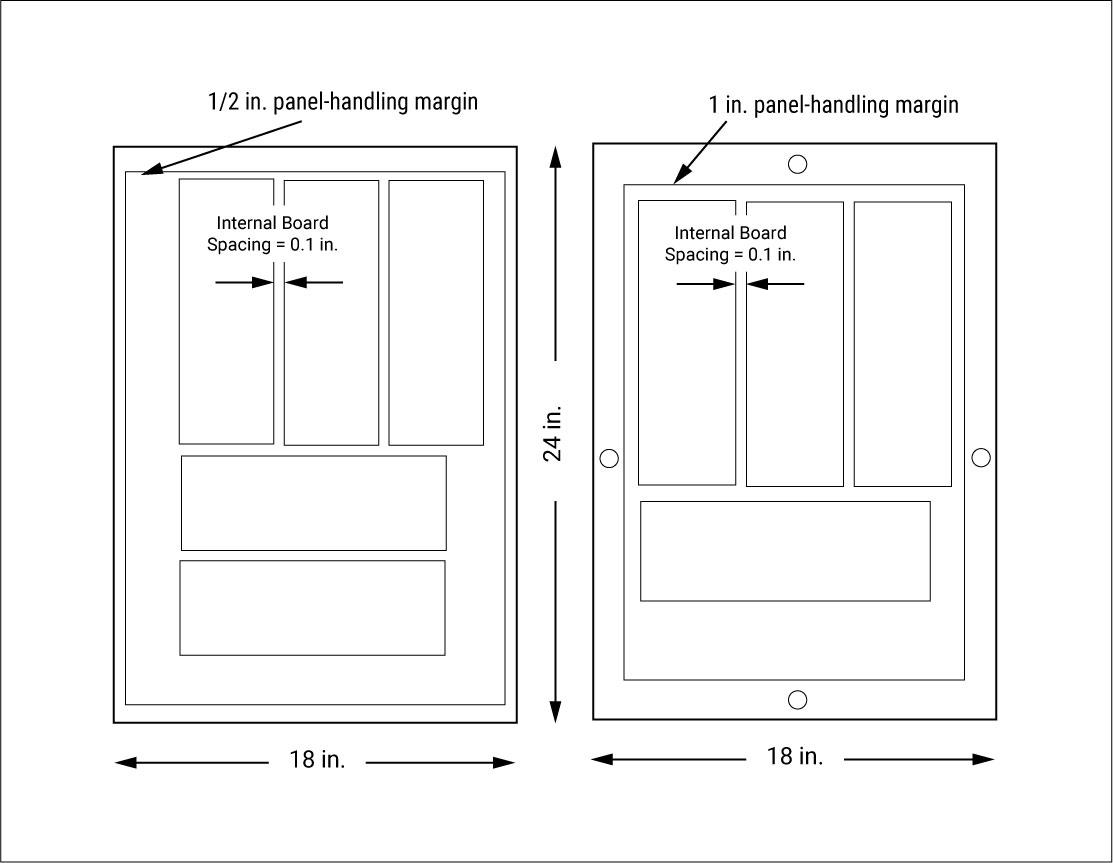
The standard sizes for PCB panels in inches are 24 x 18, 12 x 18, 24 x 9, and 12 x 9.
A perimeter clearance of half an inch (for double-sided boards) and 1 inch (for single-sided boards) is generally given. Hence the space available for placement reduces further. A routing space of 0.1 inches has to be given between individual boards placed in the panel. This space cannot be utilized for anything else.
Use a panel calculator to find out the usable space available in the panel. The same panel can have multiple boards if only the usable space is more than 70%.
Test coupons
Test coupons are small-sized replicas of PCB traces with the same layers. These are used for testing the controlled impedance of the circuit boards. Now the controlled impedance layers of the main circuit board will be very difficult to access. That is why we have to use test coupons for their testing. Generally, one test coupon is fabricated at the end of each board panel to check for the consistency of all the individual board parameters.
Types of panels for assembly
The large panels are available in different types. Below are the two commonly used panels for SMT assembly.
Single-up PCB panel
In single-up panels, only a single circuit board with a single design can be placed. These types of panels are used in cases where the size of the individual board is large. It is also used in low-volume board assemblies.
Multi-up PCB panel
Multi-up panels allow the placement of a few boards in the panel which has the same design. The number of boards that can be mounted depends on the size of the individual boards.
Size and location of fiducials
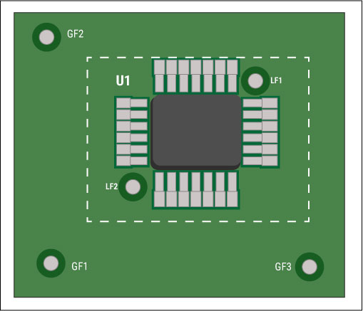
Fiducials or fiducial markers are the reference points marked on a circuit board as a reference for automated equipment.
The fiducial marks are classified into two:
- Global fiducial markers: These are placed on the edge of the board and help to identify the orientation of the PCB with respect to the X-Y axis.
- Local fiducial markers: These markers are placed on the outside edge of any quad packaged SMT component. These help the placement machines to recognize the footprint of these packages.
In the figure below GF1, GF2, and GF3 represent global fiducial markers, and LF1 and LF2 represent local fiducial markers.
Design aspects of fiducial markers
- The diameter should be between 1 to 3 mm. A clearance area similar to the diameter of the marker should be given around the marker.
- A minimum clearance of at least 3 mm should be there from the edge of the board. This is to ensure that these markers are not getting covered by conveyors or automated placement machinery/tools.
- For best accuracy, 3 global fiducials should be placed on the edges of the board.
- At least 2 local fiducials should be diagonally placed on the outside of the surface-mount component.
- Fiducials should be made by placing a non-drilled copper layer in a circular shape. These markers should not have a solder mask layer.
Tooling holes
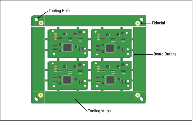
Tooling holes are present at the edges of the panels. These holes help the machines to hold the panel down for alignment. They are helpful during drilling and assembly processes where the panels need to be perfectly still.
Tooling holes are non-plated. There is no standard size for these holes. Their dimensions are completely dependent on the manufacturer and will be changed as per requirement.
The aforementioned aspects can be quite helpful while designing panels for board assembly.


