Due to the widespread focus on RoHS regulations, lead-free surface finishes are gaining a lot of popularity. One such Pb-free finish is immersion silver, which can be applied directly on copper surfaces and is ideal for EMI shielding, aluminum wire bonding, etc.
What is immersion silver finish on PCBs?
Immersion silver is an environment-friendly surface finish plated on the copper surface of a PCB to ensure good soldering of components. It is the process of depositing a thin layer (5-15 µin) of silver by a chemical reaction between silver ions and the metal copper present on the board. Currently, this surface finish is the best choice due to its outstanding performance and affordable cost. When compared to OSP and immersion gold, the silver finish process is a lot simpler and quicker.

It can maintain its electrical properties and solderability even after exposure to heat, pollution, humidity, etc. However, it will tarnish because of the absence of nickel underneath the silver. This finish lacks physical strength like immersion gold.
Fundamental concept of immersion silver
Immersion silver follows a particular sequence of steps with specific temperature, duration, and operating mode. Some of the stages are pre-treatment, acid degreasing, micro etching, etc. Among these the two crucial ones are:
- Pre-treatment – involves pickling, scrubbing, washing, and drying.
- Post-treatment – consists of washing and drying.
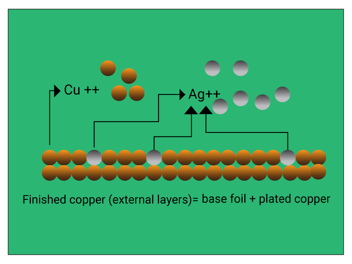
The displacement reaction of silver finish is:
2Ag+ + Cu = 2Ag + Cu++
Once the copper surface is micro-roughened with the micro etching solution, immersion silver layer is gradually plated at a controlled silver deposition rate. Immersion at a slower speed allows a dense crystal to form, resulting in a high-density layer of silver, as well as avoiding particle growth due to precipitation and agglomeration. Immersion silver solutions are stable, have a long service life, and are unaffected by light and traces of halides.

Design for Manufacturing Handbook
11 Chapters - 96 Pages - 90 Minute ReadWhat's Inside:
- Annular rings: avoid drill breakouts
- Vias: optimize your design
- Trace width and space: follow the best practices
- Solder mask and silkscreen: get the must-knows
Download Now
Advantages and disadvantages of immersion silver
The advantages include:
- Budget-friendly (less expensive than immersion gold)
- Flat surface and low contact resistance
- Good for BGA and other small components
- Strong solder connection
- RoHS compliant
The disadvantages are:
- Sensitive to handling
- When left unprotected from environmental influences, silver reacts with sulfur and forms silver sulfide on the pad.
Important points regarding silver finish
- It is easier to use than OSP.
- In contrast to HASL, it offers a more planar surface.
- For storage and handling, this surface finish needs more care than immersion tin.
- It is safer for the environment than immersion tin.
- In dry storage, this finish will last 6 to 12 months, the same as HASL boards.
- Boards with this finish must then be soldered within 24 hours once removed from storage.
- If boards with silver finish have been stored for more than 12 months, a solderability test has to be performed before assembling them.
During the immersion silver plating, some common problems may occur such as galvanic effect, solderability issue, etc. These can be rectified with proper measures. It is vital to focus on materials, handling conditions, and packaging requirements for this finish.


