Class 3 PCBs are designed and fabricated to meet stringent requirements of medical, aerospace, and military applications. Board designers and manufacturers should stick to IPC-6012 and IPC-A-610 to produce class 3 boards.
Class 3 fab notes: Things to include
- Specify the IPC-6012 addendum based on the application:
- IPC-6012 ES: Space and military applications
- IPC-6012 EM: Medtech devices
- IPC-6012 EA: Automotive industry
- Include 2 piles of prepregs.
- Voids, breakouts, and lifted rings are not allowed.
- Incorporate at least 1 mil of copper plating inside the holes to ensure reliability.
- Keep the via protrusion more than 1.96 mil and cap plating of a minimum of 0.472 mil.
- Set external and internal annular ring dimensions as 2 mil and 1 mil respectively.
- Fill 75% of the barrel for through-hole leads.
- Clearance between the pad and the copper features should be at least 4 mil.
Here, you will learn the best practices to build an efficient class 3 board, emphasizing design and manufacturing.
Key parameters:
- Material selection
- Stack-up design
- Via requirements
- Annular ring considerations
- Solder mask thickness and clearances
- Silkscreen specs
- Soldering standards
- IPC-2221 A/B and D coupons

IPC Class 3 Design Guide
8 Chapters - 23 Pages - 35 Minute ReadWhat's Inside:
- IPC guidelines for manufacturing defects
- IPC standards for assembly processes
- Common differences between the classes
- IPC documents to set the level of acceptance criteria
Download Now
Best practices and standards to build a class 3 board
The infographic below summarizes the key requirements and best practices for IPC class 3 PCB design and manufacturing.

1. Choose a material with high Tg to prevent delamination
- Select a PCB material with high Tg (>170°C) to withstand high operating temperatures. This reduces the risk of board delamination.
- Thermal conductivity should be greater than 0.4 W/m.K to ensure efficient heat dissipation.
- Opt for a smooth copper profile with a low skin effect to avoid signal integrity issues.
- For high-frequency applications, choose a material with a dielectric constant <4 to minimize signal loss.

- Pick a material with a CTE closer to the CTE of copper to eliminate stress-induced failures.
- The laminate should be CAF-resistant and RoHS-compliant to prevent corrosion from hazardous chemicals like lead, mercury, and cadmium.
2. Optimize your class 3 stack-up for signal integrity
- Maintain symmetry in your build-up to ensure uniform impedance and reduce crosstalk.
- Place the power and ground planes adjacent to each other to minimize EMI. Include the signal layer next to ground planes for shorter return paths and tighter coupling.
- If your design carries a high current (>2 amps), opt for higher copper weights (2 or 3 oz) to avoid overheating. For power and ground layers, the thickness can be 1 oz.
- Implement 2 plies of prepreg layers instead of one, to ensure reliability.
- As per the IPC-6012 standard, the dielectric thickness for a class 3 design should be at least 90 μm/3.54 mil.

3. Quality standards to build vias
- Plating voids are not allowed in class 3 boards.

- Laminate cracks within 80 μm/3.14 mil are acceptable in class 3 vias. Any cracking or separation beyond this standard can lead to conductive anodic filament (CAF) failures.
- When you have multiple sub-lams design larger annular rings to ensure accurate layer registration.
- Maintain a sufficient (10 mil) drill-to-copper distance in multiple lamination cycles.
- Add a teardrop to establish a strong electrical connection between vias and traces. This reduces the mechanical stress on the plated holes and consequently the risks of misregistration and drill breakout.

- Incorporate copper wrap plating to increase the reliability of the vias-in-pad (IPC-6012B). In capped and filled vias, the cap plating should be a min of 12 μm/0.472 mil, and the protrusion in via can’t be more than 50 μm/1.96 mil.

- Positive etch back is recommended for class 3 boards where the epoxy resin is etched back from the sidewalls of the hole using a plasma etcher. This etchant selectively removes the epoxy resin and establishes a 3-point electrical connection. The interconnects extend outward from the hole wall as shown below. This configuration enables the plating to wrap around the interconnects, creating a 3-point contact. A positive etch-back structure is more resistant to Z-axis expansion and reduces the risk of separation between the plated copper in the holes and the interconnects.

- Minimum plating thickness to design class 3 vias are as follows:
| Through, blind and buried hole (>2 layers) | Blind and buried microvias |
|---|---|
| 25 μm/0.98 mil | 12 μm/0.472 mil |
4. What is the minimum annular ring size for class 3?
The annular ring diameter differs depending on the plating thickness. For internal layers, you need to measure from the edge of the drilled hole. For external layers, calculate the diameter from the edge of the wall plating.
The minimum values for annular ring diameter are as below:
-
- 6 mil for pads on the external board layers
- 7 mil for pads on the internal layers

External and internal annular ring diameters of class 3 PCB.

An insufficient annular ring leads to drill breakout if the drill does not hit the center of the pad. According to IPC-6012, lifted/fractured rings and drill breakouts are not allowed in class 3 PCBs.

Pad size depends on the type, layer count, and annular ring dimensions. Use the following formula to calculate the pad size as per IPC-6012 and IPC-2221 standards:
Pad size = finished hole diameter + 2 (minimum annular ring size) + fabrication allowance
Keep the drill size 4 mil to 5 mil larger than the finished hole diameter to achieve the right copper plating.
Refer to the following table for class 3 drill and pad diameters for 1/2 oz. copper thickness:
| Drill | Pad | Antipad | PCB thickness | Aspect ratio |
|---|---|---|---|---|
| 0.008" | 0.023" | 0.033" | Up to 0.062” | 7.75:1 |
| 0.010" | 0.025" | 0.035" | Up to 0.100” | 10:1 |
| 0.012" | 0.027" | 0.037" | Up to 0.120” | 10:1 |
| 0.135" | 0.028" | 0.038" | Up to 0.135” | 10:1 |
For more on pad size calculation, see IPC class 2 vs class 3: The different design rules.
5. Solder mask specifications for class 3 boards
- Apply a solder mask thickness between 15 and 35 µm (0.6 to 1.4 mil). Adhesion between the solder mask and bare copper/laminate should be 100%.

- Certain areas of the PCB may have plated copper features, such as gold fingers or edge connectors. For edge fingers, open the solder mask at the finger location till the board edge. This avoids chipping off of the solder mask when inserting the boards into female connectors.

- Recommended solder mask clearances for green and other colors are 4 mil and 5 mil, respectively.

6. Have legible silkscreen texts
- Silkscreen markings should meet specific line width and spacing requirements to ensure legibility and prevent smudging during the printing process. We recommend a minimum text height of 25 mil and a minimum line width of 4 mil for silkscreen.

- Silkscreen markings should maintain a minimum of 5 mil clearance from other features such as copper traces, solder mask openings, and component pads. Adequate clearance prevents overlap and interference during the soldering and assembly processes.
7. IPC-J-STD-001 standards for soldering
- IPC-J-STD-001 states there can be no visual defects or barrel cracks.
- The required barrel fill amount for through-hole leads is 75% for class 3. Try to keep your PTH 15 mil larger than the lead diameter. Then, you will have 7.5 mil on either side, and it will be simpler to fill the paste inside the barrel.

- Imperfection along the edge of the land (pad) should not be more than 20% of the pad length. For internal pads, defects should not exceed 10% of the pad length.
- Maintain at least 4 mil of the dam between the adjacent pads after 2 mil of clearance on each side of the copper features.

- PCBs undergo thermal and mechanical stress during the reflow process. Your board should be able to withstand at least 4 thermal excursions.

Test coupons to inspect a class 3 board’s reliability
Test coupons are an efficient approach to testing the electrical connections and structural integrity of class 3 PCBs. To ensure an effective test procedure, clearly communicate your coupon requirements to your manufacturer.
Here’s what you should include in the fab notes:
- Purpose of the test coupons
- Drawing instructions (dimensions, shape, and layout of the test coupons)
- Pad sizes, trace widths, and line spacing on the coupons
- Number of test coupons and the intended locations on the PCB panel
IPC-2221 A/B coupon
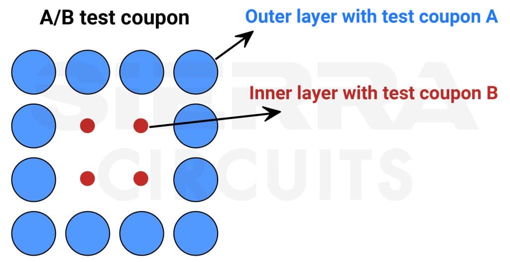
The A/B coupon inspects both vias and component holes. The outer row represents test coupon A which enables rework simulation for component holes. This coupon contains large holes with a diameter of 1.905 mm.
The inner row of this coupon holds coupon B. It assesses the thermal stress of plated-through holes. This coupon contains small holes with a diameter of 0.15 mm. Small PTHs are prone to greater tensile stress in the barrels near the central z-axis of the board.
IPC-2221 D coupon
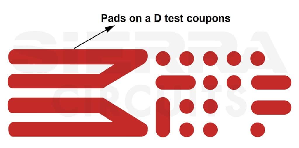
D coupons evaluate interconnection resistance, continuity, and stack-up. These coupons are placed strategically in all four corners and the center of the panel for each via structure.
To obtain precise resistance measurements, the coupon is designed with an adequate number of plated holes or vias in a daisy-chain fashion. IPC D coupons identify defects such as premature failure, plating voids, thin copper, interplane separation, cracked barrels, blind via to pad separation, and lifted lands.
IST testing with D coupons
IST subjects a coupon to thermal stress, followed by cycling electrical current through a daisy chain of vias. Furthermore, good plating integrity withstands a minimum of 300-500 cycles before any change in resistance.
Testing procedure:
- First, the D coupons are subjected to 6 reflow simulations and 100 thermal shocks, as per IPC-TM-650
- Resistance values are closely monitored every second during reflow simulation and once per cycle during thermal shocks. When there is a 10% change in resistance, via is reported as failed.
- For structures with filled vias, blind vias, and buried vias, the Propagated D coupon comes into play. This coupon may contain up to two via structures, representing multiple drilling and plating steps.
References: IPC-2221A and IPCB-2221B
Class 3 PCBs are expected to operate flawlessly in harsh conditions with extreme temperatures and vibrations. To achieve this, you need to follow the standards defined in IPC-6012ES, IPC-6012EM, and IPC-6012EA depending on your application.
Selecting a material with high Tg, maintaining symmetry in the stack-up, and adhering to annular ring specifications are some of the best class 3 PCB design practices. In addition to this, you should always consider your CM’s suggestions before finalizing the physical dimensions, clearances, and tolerance values.
For more on class 3 PCBs, download our design guide.
IPC Class 3 Design Guide
8 Chapters - 23 Pages - 35 Minute ReadWhat's Inside:
- IPC guidelines for manufacturing defects
- IPC standards for assembly processes
- Common differences between the classes
- IPC documents to set the level of acceptance criteria


