Types of vias
For the proper functioning of a PCB, different kinds of vias are required to connect various layers of the board with each other. Vias are used to connect traces on two different layers, for example, a trace running on layer one may be connected on the bottom layer of the board. This connection will be established through a via. A via is typically between 4 mil and 10mil in diameter, and its surface is covered by plated copper.
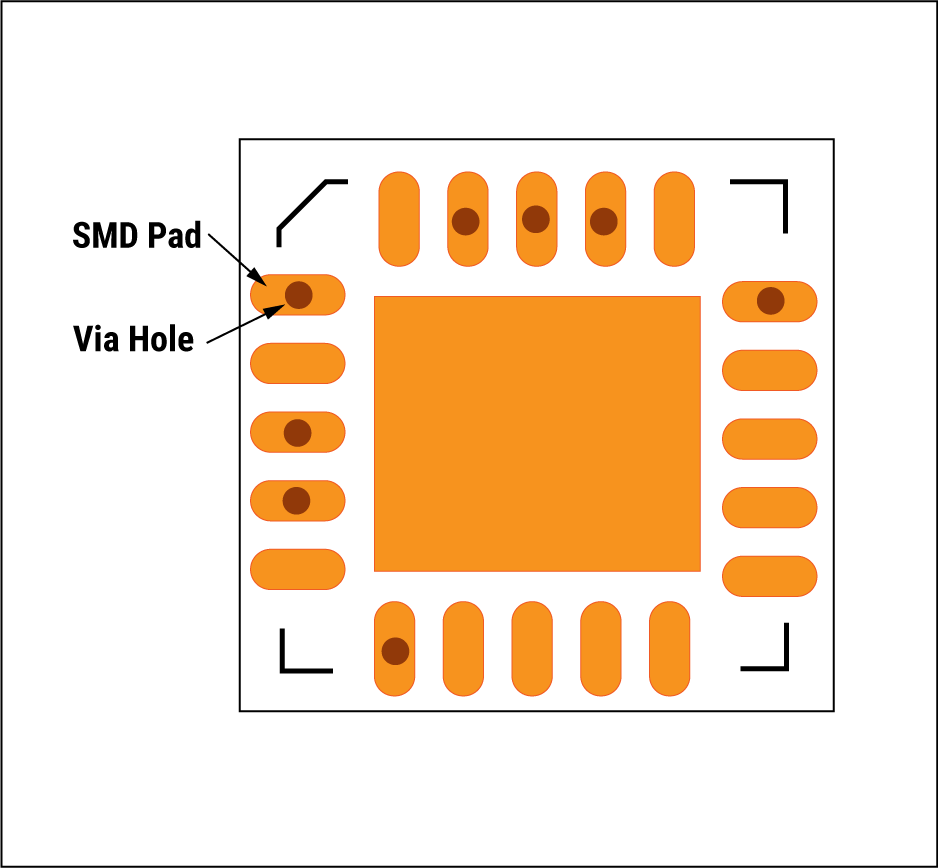
See our FAQ on via-in-pad features.
Here are a few via types:
Through-hole via
The most common type of via is the through-hole. It is a hole that is drilled through the entire thickness of the board. While it is the simplest type of via and is cost-effective, it also takes up more space on the board than other vias.
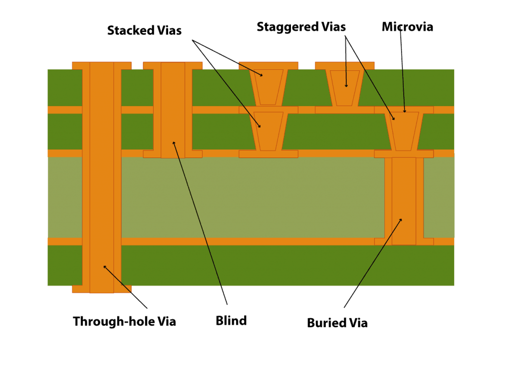
What are blind and buried vias?
A blind via always starts at an external layer and ends in an internal layer of the board.
Buried vias start and end within the internal layers of the PCB. They come at a higher cost as they are more complex to create.
Microvia
Microvias have a diameter less than or equal to 6mils that are drilled into a board with a laser. Such vias are generally used in the development of HDI boards.
[design_guide id="314"]
The most reliable PCB assembly in Silicon Valley
Avoid component procurement delays by using a single vendor to source your parts. Transparent pricing. Fast turn-times.
What is via-in-pad?
A via-in-pad (VIP) is when a via is positioned directly on a surface-mounted component pad and plated with copper. In a traditional via, the trace carrying the signal is routed away from the pad (dog-bone style) and to the via.
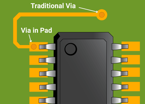
The function of a VIP is to reduce the form factor of the board, minimizing the space required for trace routing. VIPs find their application in BGA components with pitches of 0.5mm or less.
Advantages of VIP routing
VIP routing is implemented when the PCB size is limited, the components used have small footprints, and when the surface routing options are limited by design. This type of routing is conventionally utilized for BGA.
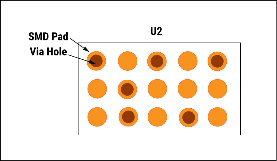
When boards are bound by design to house complex components in compact areas, board designers will place vias in the surface-mount device pads to fan out the connections. In case a design has VIP features on SMD pads, we can fill such vias with non-conductive epoxy to facilitate high-quality assembly soldering.
Design considerations for via-in-pad
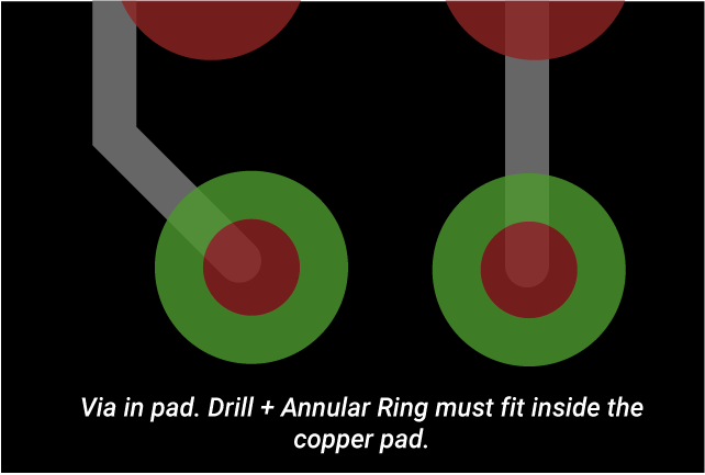
- The implementation process for VIP is almost identical to conventional vias. The difference between them lies in the design rule checks for the board. Ensure that it meets the minimum annular ring width specified by the manufacturer.
- The pad size of the component footprint needs to be equal to or larger than the minimal annular ring size. Typically, this does not pose any problems, but smaller BGA packages will need appropriate workarounds. In case the diameter of the landing pad for a BGA is smaller than the outer diameter of the annular ring, it is best to use solder mask-defined pads (SMD)
- To manufacture boards with VIPs, an extra manufacturing file is required. This is a drill file that includes the vias present in component pads, along with capping and filling. The drill file is in addition to the excellon drill file that is usually needed. Making use of two distinct files would eliminate confusion on the vias that require to be capped.
- Most VIPs need to be capped and filled, except for thermal center pads for surface-mounted power components and center pads for QFN packages. This prevents trapped gases or shifting during the reflow process.
Sierra Circuits’ engineers and technicians have the experience to bring your rigid PCBs to life.
Via filling
VIPs need to be filled and covered with copper plating. Leaving vias open exposes the plated copper to the environment and oxidation, potentially reducing the PCB’s life cycle.
The filling can be of two types:
- Non-conductive epoxy filling: Non-conductive via filling is the process of filling a via with epoxy. This technique is mostly implemented to prevent excess solder from wicking away from the pad and down into the via hole.
- Conductive filling: A conductive filling is more expensive and typically used where high current is required. The type of filling required should be mentioned in the fab notes.
The use of via-in-pads is an effective way to design boards that can house a larger number of components while dealing with a limitation on PCB real estate.
One-stop PCB assembly services, capabilities, and testing
We source components from chip manufacturers across the globe, including Mouser, Digi-Key, Arrow Electronics, and others. We also warehouse a significant inventory of common parts. If we cannot source a specific component, our engineers will make recommendations for fair-price alternatives. Get started now.


