


Contents

On-demand webinar
How Good is My Shield? An Introduction to Transfer Impedance and Shielding Effectiveness
by Karen Burnham
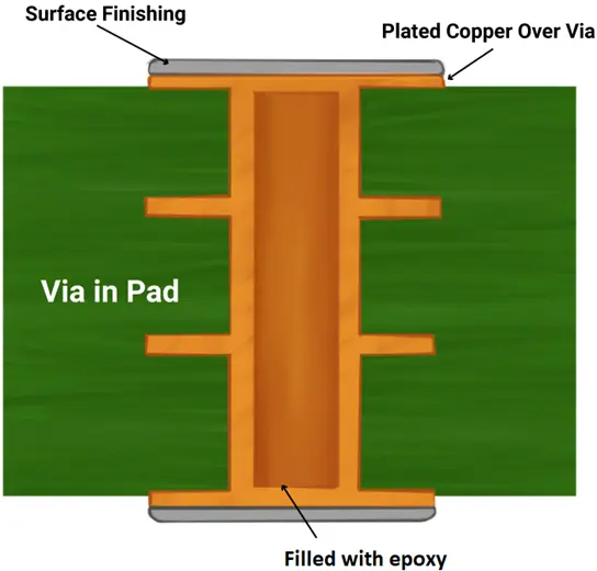
To implement via-in-pad (VIP) in your circuit boards, place the hole directly on the component pad, have it filled, planarized, and plated over to create a flat, solderable surface. This technique allows signals to transition to inner layers without consuming additional routing space.
As a PCB designer, you should choose the right via size, fill type, and pad dimensions when incorporating VIPs in your design.
Highlights:
- Via-in-pad structures enable printed board miniaturization and support the use of fine-pitch components such as BGAs.
- They simplify routing in dense layouts by allowing signals to transition to inner layers directly from the component pad.
- This technology allows you to place bypass capacitors closer to IC pins, helping reduce inductance in high-speed and power delivery networks.
In this article, you’ll learn what VIP technology is, how it differs from conventional vias, and the key design and manufacturing considerations required to implement vias-in-pad successfully in your layouts.
What are the different types of vias?
The most commonly used vias in circuit boards are through-hole vias, blind vias, buried vias, and microvias. Each type serves a specific purpose in establishing electrical connections between different layers of a multilayer board.

Before discussing via-in-pad technology, it’s important to understand these commonly used via structures.
Most PCBs contain these vias to establish connectivity between PCB layers:
Through-hole via
This is the most common via type and consists of a hole drilled through all layers of the circuit board stack-up. It is the simplest and most cost-effective option. Since it passes through the entire board, a through-hole occupies more routing space and can reduce the available area for component placement.
Blind via
It connects the outer layers of a printed board to one or more inner layers without passing through the entire stack-up.
Buried via
This hole type connects only the internal layers. Since they start and end within the inner layers, they are not visible from the outer surfaces. These holes require additional fabrication steps and, therefore, increase manufacturing complexity and cost.

Also read, PCB Via Design Using Altium Designer
Microvia
It is a very small plated hole, typically 6 mil or less in diameter, that is created using laser drilling. Microvias are commonly used in HDI designs to support fine-pitch components and dense routing requirements.

HDI PCB Design Guide
5 Chapters - 52 Pages - 60 Minute ReadWhat's Inside:
- Planning your stack-up and microvia structure
- Choosing the right materials
- Signal integrity and controlled impedance in HDI
- Manufacturing considerations for higher yields
Download Now
Vias play a crucial role in interconnection as they are used to route electrical signals between layers. Refer to our post on designing a via with current-carrying capacity to understand factors affecting via current, via fabrication types, etc.
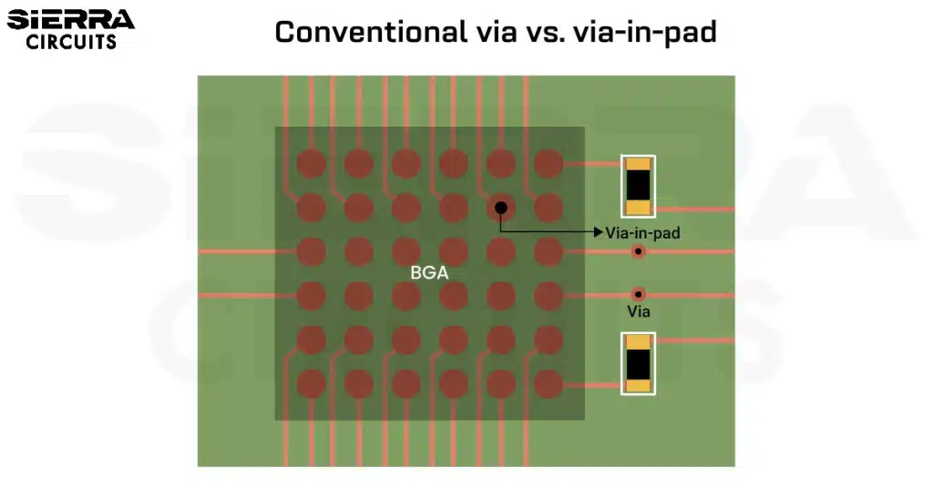
What is a via-in-pad?
A VIP is a hole placed directly on the copper pad of a surface-mounted component. The via is typically filled, planarized, and plated over with copper to create a flat, solderable surface.
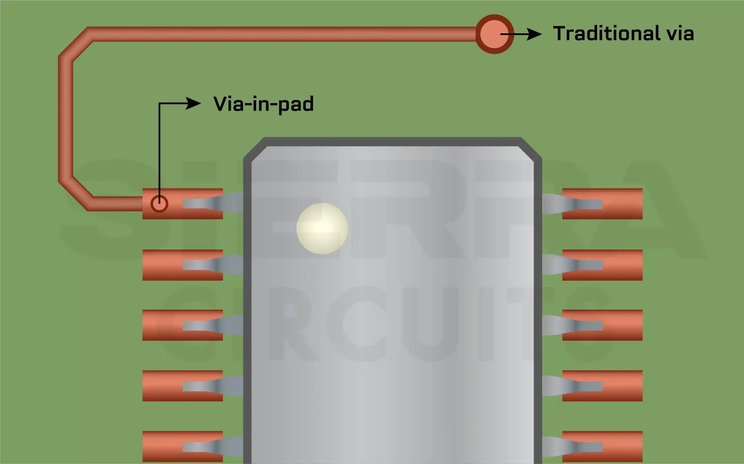
This technique differs from conventional routing methods, where a trace first exits the component pad and connects to a nearby via using a dog-bone fan-out pattern. By placing the via directly on the pad, you can eliminate the need for additional routing space, enabling more compact layouts.
This technology is commonly used with fine-pitch components such as BGAs with pitches of 0.5 mm or smaller, where traditional routing methods may not provide enough space to escape signals.
Another benefit of VIP structures is that they shorten the signal path, which helps reduce parasitic capacitance and capacitance, improving signal integrity in dense and high-speed designs.
What are the advantages of VIP routing?
Via-in-pad routing helps you create compact, high-density boards by allowing signals to transition directly from the component pad to inner layers. This approach saves routing space and makes it easier to work with fine-pitch components in dense layouts.
It is typically used when board space is limited, component footprints are very small, and routing options are restricted.
When boards feature complex devices in compact areas, you can place vias directly on SMD pads to fan out connections efficiently. In such cases, manufacturers usually fill the vias with non-conductive epoxy and plate them over to ensure a flat and reliable surface for soldering.
For more on via filling, see via filling techniques designers should know for PCB fabrication.
Compared to conventional routing techniques, VIPs offer several advantages:
- Simplifies routing for fine-pitch BGAs, especially those with pitches smaller than 0.8 mm or 1 mm (32–40 mil). To learn how to break small-pitch BGA and microcontroller using via-in-pad, see our case study on routing microcontroller and BGA in rigid-flex PCBs.

- Reduces routing distance, allowing you place bypass capacitors close to IC pins, which lowers inductance.
- Eliminates the need for dog-bone fan-out routing, freeing up surface space for additional components or traces.
- Improves high-frequency grounding by providing shorter electrical paths.

What are the cons of via-in-pad technology?
VIP routing provides significant design benefits, but it introduces additional manufacturing complexity.
- The fabrication process requires extra drilling, via filling, planarization, and copper plating steps, which increases manufacturing time and cost.
- Manufacturers must ensure the via surface is perfectly planar to avoid bumps that can affect BGA solder joints.
- Outgassing may occur during soldering. It refers to vapor expansion inside the via during heating, which can create voids or bubbles in solder joints, affecting assembly reliability.
Vias vs. via in pads
| Feature | Conventional via | Via-in-pad |
|---|---|---|
| Via location | Near the component pad and connected using a short trace (dog-bone routing) | On the component pad |
| Solder flow control method | A solder mask plug or tenting is used to prevent solder from flowing | The via must be completely filled and capped to prevent solder wicking |
| Via filling | Typically left open or tented with solder mask | Usually filled with non-conductive epoxy or copper and then plated over |
| Surface planarity requirements | Flat surfaces are not always required | Requires planarization and copper capping to create a flat surface for reliable soldering |
| Assembly reliability | Less critical because solder does not sit directly over the via | A flat, void-free surface is essential for reliable solder joints, especially for BGAs |
| Manufacturing complexity | Low | High |
| Typical applications | Standard circuit boards with sufficient routing space | High-density PCBs, fine-pitch BGAs, and compact designs |
Mechanically drilled via-in-pad holes, as stated, need to be filled with epoxy. The choice of epoxy depends largely on the coefficient of thermal expansion (CTE) of the via-in-pad fill material and the laminate used. This is important because, as the PCB undergoes heating and cooling phases during stack-up, the fill material will move with or against the surrounding laminate board material. It can cause stress-induced fractures and even electrical circuit breaks.
Since non-conductive epoxies have CTEs that are a closer match to that of laminates, you choose them often. This is also a cost-effective option as well. The design and intent of a PCB will ultimately decide the type of epoxy that is required for a via fill.

Importance of pad dimensions in VIPs
The pad diameter of the component footprint plays an important role in determining the manufacturing method used for via-in-pad structures.
To comply with IPC class 2 or class 3 annular ring requirements, the pad must be large enough to accommodate:
- The via diameter
- The required annular ring
- Manufacturing tolerances
When using mechanical drilling, you must consider the drill size (pre-plating drill diameter) and the remaining annular ring after copper plating.

IPC Class 3 Design Guide
8 Chapters - 23 Pages - 35 Minute ReadWhat's Inside:
- IPC guidelines for manufacturing defects
- IPC standards for assembly processes
- Common differences between the classes
- IPC documents to set the level of acceptance criteria
Download Now
3 design guidelines for routing vias-in-pad
If your design requires VIP structures, you should follow certain practices to reduce manufacturing challenges and avoid unnecessary cost and fabrication time.
Stick to the following layout guidelines:
- Follow the part manufacturer’s recommendations when placing components, via capping, and via filling.
- Cap the via on the non-component side with solder mask to protect the copper surface.
- Avoid leaving vias open unless absolutely necessary. Open vias can expose the copper to the environment, leading to oxidation and potential reliability issues that may shorten the board’s lifespan.
Sierra Circuits’ via-in-pad capabilities
We manufacture VIP structures with a minimum diameter of 6 mil.
Common devices that require holes on pads include BGAs, QFNs, and surface-mount components such as resistors, capacitors, ICs, and connectors.


In certain cases, you don’t have to fill vias. In these scenarios, you don’t need to mark them as via-in-pad in your fab drawings.
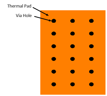
Thermal pads don’t require soldering.


Key takeaways:
- Via-in-pad pad size must consider both via diameter and IPC annular ring requirements (Class 2 or 3) for solder integrity, isolation, and manufacturability.
- Opt for fully filled via-in-pads (epoxy or copper) on a flat surface for reliable BGA placement.
- You can skip via-plugging for via-in-pad designs. Since it’s located under the component, it naturally prevents solder wicking.
Electronic components are always shrinking in size, and hardware engineers will need to learn and use innovative tools and techniques to install these components in a way that is scalable and reliable. Via-in-pad technology is a great step towards innovative PCB build techniques.
Need assistance in designing via-in-pads in your design? Post your queries on our forum, SierraConnect. Our design experts will resolve them.

About Milan Yogendrappa : Milan Y is an electronics and communication engineer with over 6 years of experience in developing and editing technical articles related to PCB design, manufacturing, and assembly. He is currently the editor-in-chief at Sierra Circuits.


Start the discussion at sierraconnect.protoexpress.com