What are heavy copper PCBs?
Printed circuit boards carry current through etched copper tracks. The current carrying capacity of a copper trace can be improved by increasing its width, but this is not always practical. Another way to increase the current carrying capacity without changing the width of the copper traces is to use heavy or thick copper. This carries more current and enhances efficiency with better heat management.
There are no definite rules that specify the amount of copper to be used when fabricating heavy copper boards. However, the PCB industry considers 3 or more ounces of copper on any circuit board layer as heavy copper.
Note: Sierra Circuits offers up to 5 oz copper.

Design considerations for thick-copper boards
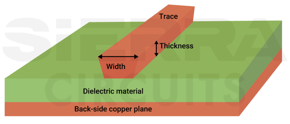
Copper thickness and width
PCB designers gauge the amount of current required, and based on this, they design their heavy copper boards. This involves selecting the right copper thickness, width, and the maximum temperature rise the circuit board can withstand. The amount of heat a heavy copper board generates is proportional to the amount of current it carries.
How to choose the right copper thickness
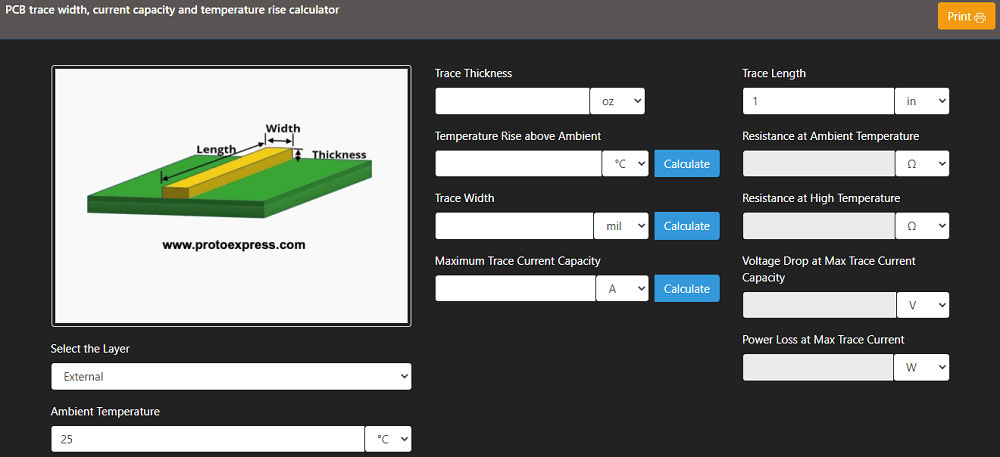
As stated earlier, the copper thickness is determined by the current passing through the conductor. The thickness of the board can be determined by a trace width calculator. It can calculate the three parameters that include trace width, current capacity, and temperature rise. If any two parameters are known, the tool calculates the third.
Current carrying capacity
As current passes through a copper trace, its resistance inadvertently heats it up. The local heat transition generates a power that dissipates into the atmosphere by conduction and convection. The designer must calculate the maximum current the trace can carry before it reaches the acceptable temperature rise of about 30°C. A thumb rule in the industry is that the inner layers can sustain only 50% of the current-carrying capacity of the exposed traces.
Substrate material
The substrate of a PCB is another factor a designer should consider while designing heavy copper boards. Substrate materials range from ordinary FR-4 material with operational temperatures of 130°C to advanced materials with very high glass transition temperatures (Tg). The Tg of the copper and substrate material is very critical since a high current may cause cracks and layer separation.

PCB Material Design Guide
9 Chapters - 30 Pages - 40 Minute ReadWhat's Inside:
- Basic properties of the dielectric material to be considered
- Signal loss in PCB substrates
- Copper foil selection
- Key considerations for choosing PCB materials
Download Now
Coefficient of thermal expansion (CTE)
Coefficient of thermal expansion (CTE) is the rate of expansion of a PCB material as it heats up. It is expressed in parts per million (ppm), expanded for every degree Celsius that it is heated to. CTE between copper and the substrate material is also important, as thermal stress produced by high currents through traces may result in the formation of cracks, eventually causing board failure.

Circuit board surface thickness can be elevated through electroplating. It reduces the resistance of copper traces through the improvement of heat conduction. Fabricators also use electroplating for PTHs to minimize their thermal resistance. Resistance reduction helps to dissipate heat efficiently through the modes of heat transfer, such as conduction, convection, and radiation.


