


Contents
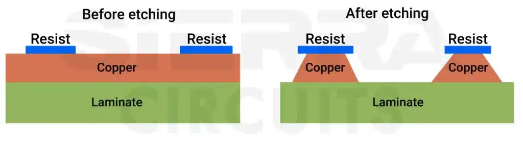
Wet PCB etching is a process of removing unwanted copper by immersing a circuit board in a chemical solution (acidic or alkaline-based). Since the entire board is submerged in the chemical solution, the corrosion is uniform in all directions.
What is PCB etching?
PCB etching is a process of removing unwanted copper (Cu) from the circuit board to achieve the desired circuit pattern.
In other words, etching is like chiseling the circuit board. If you can think like an artist, the board is a rock, and etching chisels the rock into a beautiful sculpture. During this process, the base copper or the start copper is removed from the board. Rolled and annealed copper is easy to etch off compared to electroplated copper.
Before the process of etching, a circuit board layout is prepared so that the end product is as per the designer’s requirements. The designer’s desired image of the circuit is transferred onto a PCB by a process called Photolithography. This forms the blueprint that decides which part of the copper must be removed from the board.
There are two distinctive approaches for the inner layer and outer layer etching. In the outer layer etching process, the tin plating acts as the etch resist. Whereas, in the inner layer, the photoresist is the etch resist.
PCB etching can be done using two methods: wet etching and dry etching.

What factors should you consider before choosing a PCB etching process?
The direction, rate, and selectivity of etching significantly impact the final PCB quality. Before starting the etching process, evaluate the following factors:
Direction of etching
To have a controlled rate of etching, you need to choose the appropriate direction of the etching. There are two categories:
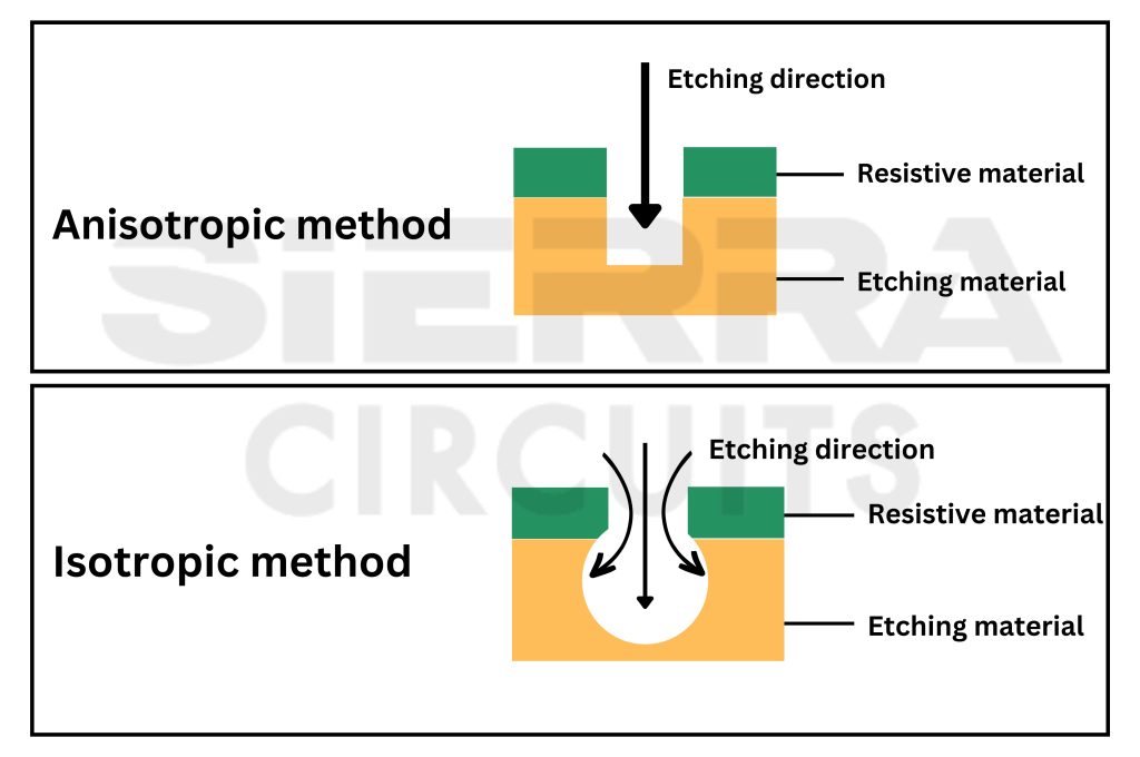
Anisotropic: This process removes material along a particular or designated direction. This method is employed in the dry etching process, and the etching rate can be controlled.
Isotropic: In this process, the etching rate is constant in all directions. Wet etching is an isotropic method. But, in this process, controlling the rate of etching is challenging.
Selectivity of etching
Selectivity can be defined as the ratio of etch rates between materials. It is essential to understand etch selectivity to accurately calculate the mask thickness and control the etching process.
How is wet PCB etching carried out?
Wet PCB etching removes unwanted copper by exposing the board to liquid chemical etchants, typically acid- or alkaline-based solutions. During the process, the etchant reacts with the exposed copper and dissolves it from the PCB surface.
This procedure is widely employed in microelectronic applications. The quality of the etching process mainly depends on:
- Chemical characteristics of the etchants
- The concentration of the etching solution
- Temperature and pressure
- Equipment configuration
Chemical reactions during the wet etch process include:
- Diffusion: Liquid etchant is diffused into the region that is to be eliminated.
- Reduction-oxidation: This reaction occurs between the liquid etchant and the material that is being etched away.
- Residue removal: The by-products are diffused from the reacted surface.

Design for Manufacturing Handbook
11 Chapters - 96 Pages - 90 Minute ReadWhat's Inside:
- Annular rings: avoid drill breakouts
- Vias: optimize your design
- Trace width and space: follow the best practices
- Solder mask and silkscreen: get the must-knows
Download Now
What are the different methods of wet PCB etching?
The two main methods of wet PCB etching are acidic etching and alkaline etching. Both remove unwanted material using chemical solutions, but they differ based on the type of etchant used.

- Acidic etching: Uses ferric chloride or cupric chloride solutions.
- Alkaline etching: Uses ammoniacal etchants.
Both these methods have their own pros and cons.
How does the acidic PCB etching process work?
The acidic PCB etching process removes unwanted copper from the inner layers using chemical etchants such as ferric chloride (FeCl₃) or cupric chloride (CuCl₂). PCB manufacturers prefer this method for inner layers because it offers high precision, minimal undercuts, and does not attack the photoresist.
This procedure is more precise and cheaper but time-consuming, compared to the alkaline method. It is implemented for the inner layers because the acid doesn’t react with the photoresist and doesn’t damage the required part. Also, the undercuts are minimal when you use this technique.
Undercuts are the lateral erosion of the etched material below the protective tin/lead layer. When the solution hits the copper, it attacks the copper and leaves behind the tracks that are protected. The tracks are protected with either a plated etch resist or a photo-imaged resist. At the track edge, there is always some amount of copper removed under the resist; this is known as an undercut.

Let’s take a quick look at the two main types of acidic etching.
Cupric chloride etching process
In this process, the PCB is exposed to a cupric chloride-sodium chloride-HCl solution that dissolves the unwanted copper. The chemical system also supports continuous regeneration, making it a cost-effective option for high-volume manufacturing.
Cupric chloride is the most widely used etchant since it accurately etches off smaller features. This process also provides a constant etch rate and continuous regeneration, comparatively at a lower cost.
The maximum etching rate from the cupric chloride system is obtained from a combination of cupric chloride-sodium chloride-HCl systems. This combo gives a maximum etching rate of 55s for 1oz copper at 130°F. Hence, this type of etching is used to etch fine lines in the inner layers
Note: The use of chlorine gas requires adequate ventilation, tank and cylinder storage, and leak-detection equipment. Furthermore, it requires emergency protocols, personal protective equipment, trained operators, and approval from the fire department.
Ferric chloride etching procedure
The ferric chloride etchant has limited usage in the industry because of the costly disposal of the copper-containing etchant. However, ferric chloride is an attractive spray etchant because of its ease of use, holding capacity for copper, and ability to be used in infrequent batch applications. Ferric chloride can be used with screen ink, photoresist, and gold patterns, but it cannot be used with tin or tin/lead resists.
Usually, a ferric chloride solution is dissolved in water with a concentration ranging from 28 – 42% by weight. HCI (up to 5%) is also mixed with this solution to prevent the formation of insoluble precipitates of ferric hydroxide.
The specific gravity of ferric chloride usually used is 36 Be, or approximately 4.0lb/gal FeCl3. The acid (HCL) content will be within 1.5 to 2% for commercial purposes.
What are the steps involved in the alkaline PCB etching process?
During this procedure, the PCB moves through a conveyorized high-pressure spray chamber where a continuously refreshed etchant spray dissolves the exposed copper. The chemical composition typically includes cupric chloride (CuCl₂·2H₂O), hydrochloric acid (HCl), hydrogen peroxide (H₂O₂), and water (H₂O).
The alkaline method is a fast process and is a bit expensive as well. The parameters for this process must be diligently followed since the solvent can damage the board if it is in contact for a longer period. The process must be well-controlled.
The point at which the etching of the unwanted copper is complete is called the breakpoint. This is usually achieved at the midpoint of the spray chamber. For example, considering the spray chamber length is 2 meters, the breakpoint will be achieved when the board reaches the midpoint, i.e., 1 meter.
What are the different ways of wet PCB etching?
The two commonly used wet PCB etching techniques are the dip technique and the spinning/spraying technique. Both methods remove unwanted copper using chemical etchants, but they differ in how the etchant is applied to the PCB surface.
Dip technique: The substrate is immersed in the chemical solution, and it is retained until all the unwanted layers are removed.
Spinning and spraying technique: In this procedure, the substrate will rotate, and the etchant is sprayed in parallel. The spinning of the substrate provides a more even etch surface. The effectiveness of the process depends on:
- Type of chemical etchant
- Temperature and concentration of the solution
- The spin speed of the substance
Which parameters affect the quality of PCB etchants?
Baumé, temperature, oxidation-reduction potential (ORP), chemical additives, and pH are the key parameters that affect the quality and performance of circuit board etchants. These factors determine the etch rate, line resolution, chemical stability, and overall process consistency.
Let’s see each of these in detail.
Baumé (Bé)
Baumé is the concentration of molarity of the etchant, which depends on the specific gravity of the etchant.
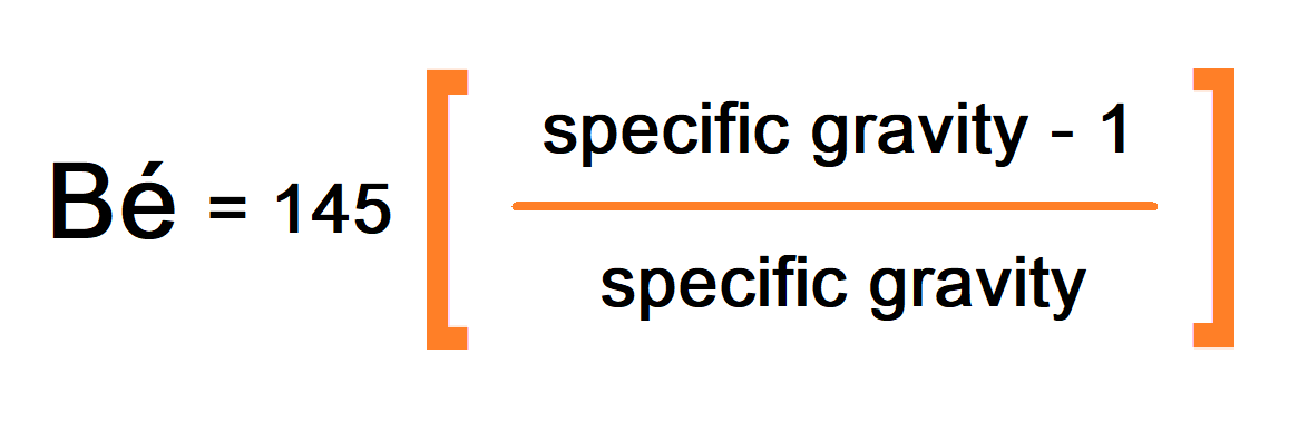
The higher the Bé value, the higher will be the molarity of the etchant, hence the etching rate of the solution. A lower Bé value would give a low etch rate with poor line resolution,n and a higher etchant would produce a slow etch rate. Undercut also decreases with the increase in Baumé value.
Temperature
In general, at high temperatures, the etch rate will be higher. But the selection of etching temperature depends on the etching machine used. Most of the etching machines use plastic parts because all metals are reactive to etchants. Hence, the etching temperature cannot be too high. The maximum etching temperature range allowed is 50-55°C.
Oxidation-reduction potential (ORP)
The measurement of ORP indicates the activity of the etchant. It is the measure of the relative conductivity of the etchant and is expressed in millivolts. The ORP indicates the relationship between cupric ions and cuprous ions or ferric ions and ferrous ions.
As the copper is etched, the etchant changes from a cupric/ferric to a cuprous/ferrous state. The higher the value of ORP, the more efficient the etchant will be, while low values of ORP indicate a slow and inefficient etchant.
Manufacturers will maintain ORP at a high constant value to achieve a constant etch rate of the metal. ORP value is influenced by free acid content and etchant temperature. The addition of free acid and oxidizer to the etchant produces free chlorine. This makes cuprous ions return to cupric form.
Adding chemical additives (Free acid)
Chemical additives are used in commercial etchants to increase the etch rate. HCI is the commonly used additive for CuCl2 and FeCl3 etchants. HCI is the source of chlorine, forming metal chlorides instead of hydroxides, which enhances the etchant’s ability to hold dissolved metals.
Additives are very important for the continuous etching process. They are added before the first use of the etchant or at regeneration. The pH value of the solution is evaluated to check the acidity of the solution.
The addition of additives increases the complexity of etchants but provides a higher etching rate. It also increases the dissolving capacity of the etchant. The addition of additives increases the etch rate, but the concentration of additives depends on the machine used. The high HCl addition causes the acid to react with the etching machine parts.
pH value
The pH value is a very important parameter in the etching process, especially for alkaline ammonia etching. It is between a range of 7.9 and 8.1 for reliable alkaline etching. Low pH below 8 can be caused by low ammonia, excessive ventilation, heating, etc.
In such cases, pH can be raised by adding anhydrous ammonia. A higher pH value above 8.8 also causes a low etch rate. This can be caused by under-ventilation, higher copper content, or water in the etchant.
In the case of acid etching methods, the pH value is used in solution control. An increase in pH leads to incorrect readings of the copper colorimeter caused by solution turbidity.
The table below summarizes important characteristics of different PCB etchants.
| Parameters | Alkaline etch | Cupric etch | Ferric etch |
|---|---|---|---|
| Temperature (°C) | 43-55 | 50-54 | 43-49 |
| Specific gravity | 1.170 | 1.34 +/-0.02 | 1.4 |
| Baumé, Be° | 25-27 | 32-33 | 36 |
| Etch rate µm/min | 30-60 | 25-50 | 25-50 |
| Dissolved copper capacity | 140-170 | 120-140 | 40-60 |
| Operational cost | High | Low | Medium |
| pH | 8.0-8.8 | NA | NA |
What is continuous etching and regeneration?
Continuous etching is an automated PCB etching process that continuously feeds fresh etchant into the system to maintain stable etching conditions. Etchant regeneration is the process of recycling and restoring used etchant so it can be reused in the etching cycle.
As the copper is dissolved in the etchants, the etchant’s density increases. To evaluate the volume of copper in a solution, the density of the etchant in the etcher is measured. When an upper limit of density is recorded in the density sensor, a switch activates a pump. The pump automatically feeds etchants into the etcher. At the same time, the system eliminates waste etchant.
For uninterrupted production in such systems, the regeneration of the etchant is an important factor.
The regeneration processes for waste etchants have been developed to solve the waste problems of the etching industry. The use of the regeneration process would also bring other benefits. Like saving equipment and operation costs, and significantly reducing liabilities associated with the disposal of hazardous waste etchant.
See the future of PCB etching by Laurent Nicolet for expert insights into PCB etching.

PCB Design for Assembly Handbook
6 Chapters - 50 Pages - 70 Minute ReadWhat's Inside:
- Recommended layout for components
- Common PCB assembly defects
- Factors that impact the cost of the PCB assembly, including:
- Component packages
- Board assembly volumes
Download Now
What are the pros and cons of wet PCB etching?
Pros:
- Can be conducted in a normal atmospheric environment
- High etching rate
- High selectivity: Wet etching can be used to etch off a wide range of materials
- Ease of equipment maintenance
- Creates a uniform surface
Cons:
- Inadequate power to etch traces less than 1μm
- High use of chemicals results in hazardous waste
- Increased risk of ionic contamination
- Direct exposure to liquid and fumes
- Resistive elements may lose their bonding to the substrate
Difference between wet etching and dry etching
| Wet etching | Dry etching |
|---|---|
| Liquid-based process | Plasma-based process |
| Chemicals in the liquid phase | Chemicals in the gaseous phase |
| Quick and preferred for bulk processing | Comparatively slower |
| High etch rate | Comparatively lower etch rate |
| Lower installation cost: requires simple equipment like baths or wet chemical sprays | Higher installation cost: requires high-end equipment like vacuum chambers |
| High maintenance due to the replenishing and disposal of chemicals | Lower maintenance as less hardware modification is required over time |
| Less safe due to the involvement of hazardous chemicals | More safer as fewer hazardous chemicals are involved |
| Lower precision | High precision |
| Isotropic process | Anisotropic process |
| Messy working environment | Cleaner working environment |
After the etching process, the end product will have the circuitry as per the designer’s specifications. Soon after the etching is completed, the board will be further processed for stripping. The stripping process removes the electroplated tin or tin/lead or the photoresist from the surface of the board.
So, this is the inside story about how the etching process takes place in a PCB manufacturing unit. We also covered different parameters that a manufacturer must monitor when etching. Hope this article scratches your itch for etching.

Quote and order your circuit boards online with our Turnkey PRO tools in just a few minutes.
About Rahul Shashikanth : Rahul Shashikanth is an electronics and communication engineer with over 8 years of experience in publishing technical articles on PCB design, manufacturing, and assembly. He is currently the content marketing manager at Sierra Circuits.


Start the discussion at sierraconnect.protoexpress.com