PCB routing gets extremely complicated when a ball grid array (BGA) component is present on the board. BGAs feature a large number of pins that are very difficult to access. Hence, the routing of these components requires a special set of instructions that do not apply to the other parts of the board. Let’s have a look at the BGA fanout process.
What is BGA fanout?
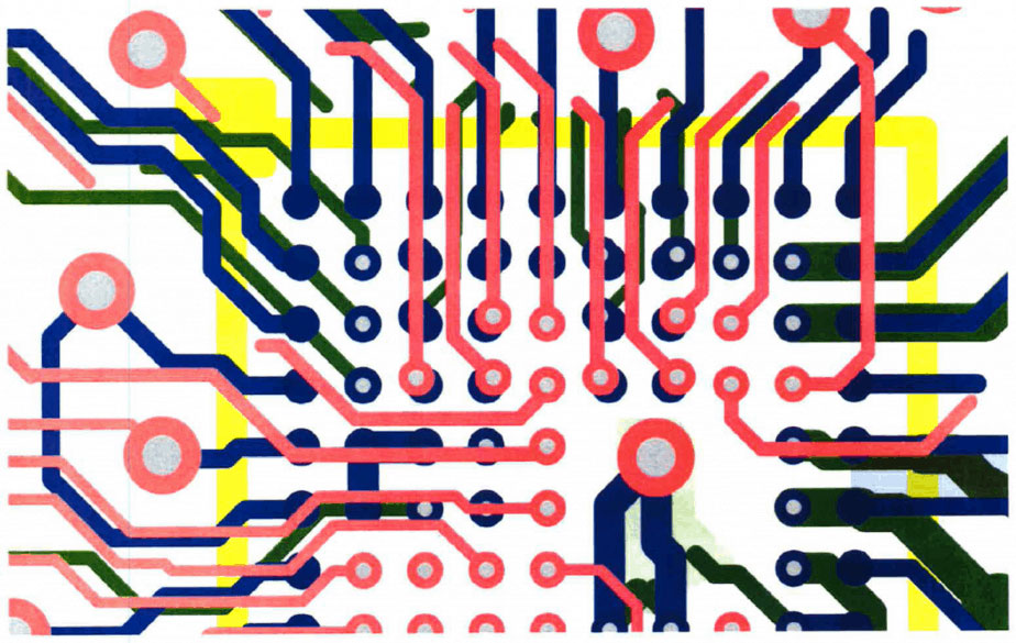
BGAs always affect the trace width, layer count, and via styles of a circuit board. These components come with extremely small pitches like 0.3 mm, 0.4 mm, 0.5 mm, etc. This makes the routing of signals from the BGA pins an extremely difficult task. Therefore, you should always have a good strategy to route the signal from the BGA pins. This process of routing the signals outside the BGA is called fanout or breakout.
BGA pitches and their impact on fanout
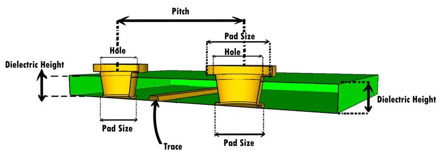
BGA pitch is defined as the distance between two adjacent solder balls measured from center to center. With the increase in the number of pins, there is a reduction in the pitch of the component. This reduction in pitch complicates the fanout solution. Thus, more internal layers should be added to route the pins, which will in turn increase the cost of PCB fabrication.
Due to these reasons, deciding the number of layers required is a tough job. There is an empirical formula that can be used to decide the number of layers.
No. of layers = Total number of signals from BGA chip / (4 sides × Routing signals from BGA per side)
To make your job easier, Sierra Circuits have introduced a tool called Stackup Designer that enables you to design a cost-effective and manufacturable layer stack.
You just have to select the appropriate BGA pattern and enter the pitch and pin information to view your stack-up options.
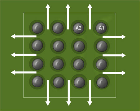
The number of traces that can be taken out from in between the peripheral pins depends on the BGA pitch. One or two traces can be routed out depending on the pitch. The number of layers required for different pin counts and pitch is given below in the table:
| BGA pins ball | Pitch in mm | Signal layer counts |
|
|---|---|---|---|
| 2 trace | 1 trace | ||
| 256 | 1 | 2 | 3 |
| 324 | 0.8 | 2 | 3 |
| 484 | 0.8 | 3 | 4 |
| 484 | 1 | 2 | 4 |
| 625 | 0.8 | 3 | 4 |
| 676 | 1 | 3 | 5 |
| 784 | 0.8 | 4 | 5 |
| 900 | 1 | 3 | 5 |
| 1156 | 1 | 3 | 6 |
| 1517 | 1 | 4 | 7 |
| 1760 | 1 | 4 | 8 |
| 1924 | 1 | 4 | 8 |
| 2577 | 1 | 5 | 9 |
| 2892 | 1 | 5 | 10 |
You can see an example of routing a 0.4mm BGA component here, how to break out a 0.4mm BGA.
Via-in-pads in BGA routing
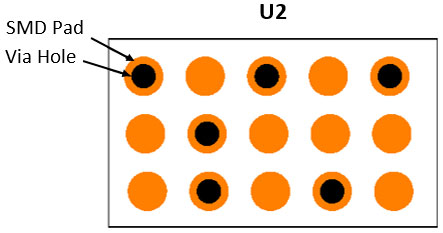
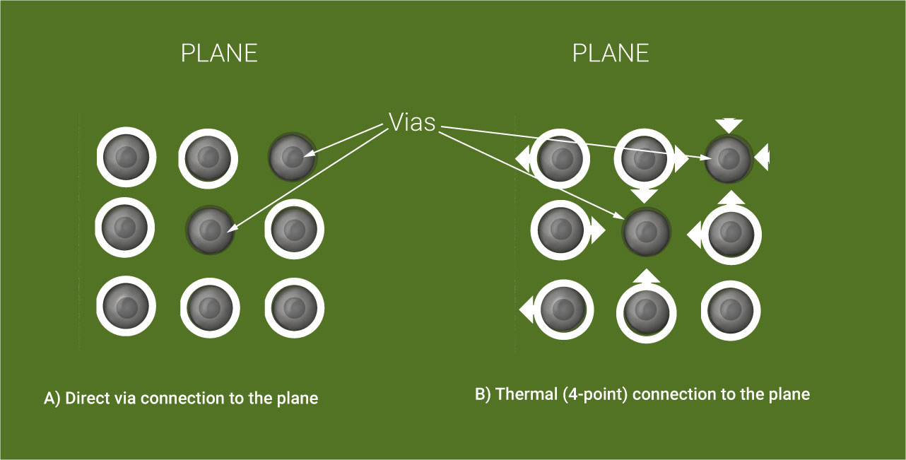
Via-in-pad method helps in routing fine-pitch BGA components. The placement of vias in the component copper landing is called via-in-pad. This technique gives more space to route the traces without design rule check (DRC) errors.
In BGA fanout, the vias are placed in pads at a certain angle to maximize the space. Mostly offset via-in-pads are used. These are VIPs placed near the border of the pads.
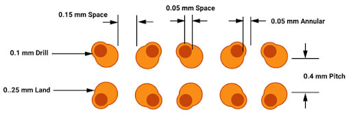
Compared to microvias in the center of the pad, using offset vias increase the space available for routing, as seen in the figure above.

HDI PCB Design Guide
5 Chapters - 52 Pages - 60 Minute ReadWhat's Inside:
- Planning your stack-up and microvia structure
- Choosing the right materials
- Signal integrity and controlled impedance in HDI
- Manufacturing considerations for higher yields
Download Now
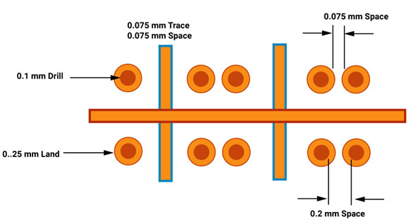
Routing traces in between pins
Traces can be routed through the closely spaced pins in different ways. As mentioned earlier, the space available to route the traces will depend on the BGA pitch.
What is neck-down in fanout routing?
When going in between the pins of a BGA, we cannot use the traces with the same width as that of the rest of the board. The width of the traces going into and coming out of the component have to be trimmed down due to the low pitch. This reduction in the track width that allows routing in tighter spaces is called neck-down. You can easily apply these rules through constraint settings.
It should be noted that this reduction should always be within DRCs and fabrication limitations.
The example shown below is the case of a 0.5 mm fine-pitch BGA component. A single trace can be taken out from the top layer without DRC errors. This allows a trace of 3 mil width in between the pads. The pad-to-trace distance will be 3 mils. Now this paves way for the possibility of taking two traces with 3 mils width from the second layer, maintaining a pad-to-trace width of 3 mils.
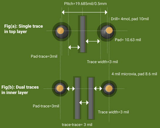
Read how to breakout a .5mm bga, for more details.
Creating a fanout solution
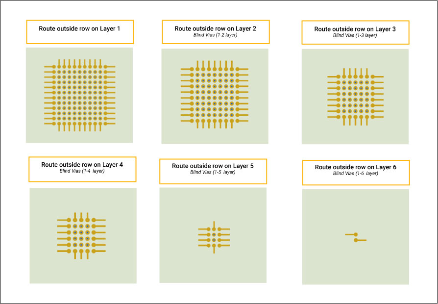
By simply using the neck-down method, we cannot access all the pins of the component. Careful planning should be involved. We know that the pins (solder balls) under a BGA have a matrix arrangement. All the pins of the fine-pitch components will be very close to each other. Therefore, only the outermost layer and sometimes the layer adjacent to it can be connected directly to the copper traces available on the board surface.
To connect the remaining BGA pins, you have to use different layers connected through the blind and buried microvias. These pins will be connected to the microvias using small traces and then those traces will carry the signals to the corresponding layers. This routing process can be executed in several different methods.
An example of this pattern is shown below. Here the outermost pads are routed directly without vias. The second row is connected to the second signal layer through blind vias and then the traces are taken out. The third row is connected from the top layer to the third signal layer using blind vias and then the traces are taken out, and so on. In this example, microvias are placed at the center of the pads. Here you will require 6 layers for routing all the pins.
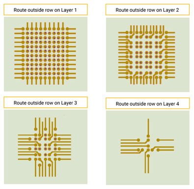
Now for the same case, if we use offset via-in-pads, then it would be as shown below. We can see that the number of layers required while using this technique is lesser than the one above.
BGA power pad routing
In some BGA packages like microprocessors, there are many power and ground pins for different voltages. These pins are usually placed on the peripheral rows or in the center. When routing these power pins, we usually use a short trace between the pin and the via.
These are the basics that you need to understand about BGA fanout. These aspects can be implemented when routing the traces out of a BGA component. But every BGA component will require different fanout strategies. With every fanout solution, you need to check that the DRCs are not violated. Only then a fanout solution can be adapted.


