Speak to an Account Manager
![]() +1 (800) 763-7503
+1 (800) 763-7503
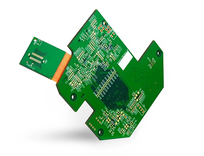
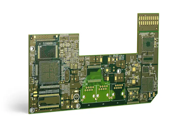
An experienced mil-spec PCB manufacturer for aerospace and defense
As a seasoned mil-spec PCB manufacturer specializing in aerospace and defense applications, Sierra Circuits takes pride in supporting those who serve our nation. Our commitment is reflected in our priority scheduling system, ensuring fast-track production for every mil-spec board we manufacture.
- Next day for standard FR-4 or double-sided PCBs
- 2–4 days for 4-layer to 8-layer PCBs
- 5 days for 10-layer PCBs and above
- 5–10 days for HDI, rigid-flex, flex, and metal core PCBs
- IPC class 3/FS

High-reliability and fast turnaround times for your defense and space board
For standard FR-4 or double-sided PCBs, our efficient production pipeline allows for next-day delivery, providing a swift turnaround to meet urgent project requirements. In the case of 4-layer to 8-layer PCBs, we maintain a turnaround time of 2–4 days, combining speed with precision to accommodate the complexity of these designs. For higher-layer configurations, such as 10-layer PCBs and above, our dedicated team ensures a prompt 5-day turnaround to keep your projects on schedule.
When it comes to advanced technologies like HDI, rigid-flex, flex, and metal core PCBs, we extend our commitment to excellence with a 5–10 day turnaround. This enables us to deliver these intricate and specialized PCBs within a reasonable timeframe, meeting the stringent requirements of aerospace and defense applications.
At Sierra Circuits, our focus is not only on manufacturing high-quality mil-spec PCBs but also on providing expedited services that align with the critical timelines of aerospace and defense projects. With our reliable and swift production capabilities, we stand as a trusted partner for those who require precision, reliability, and efficiency in every mil-spec PCB we deliver.

Sierra Circuits supports IPC-2581.
In the manufacturing landscape of printed circuit boards, IPC-2581 stands as a crucial standard for the seamless exchange of design data. This open, vendor-neutral XML format plays a vital role in navigating the intricacies of PCBs, facilitating clear communication regarding layer stack-up, drill details, and other critical specifications. Adhering to IPC-2581 becomes paramount for mil-spec PCB designers and manufacturers to ensure transparent data exchanges, effectively minimizing the likelihood of errors during the process. Embracing this standardized approach not only promotes improved collaboration but also streamlines workflows, significantly contributing to the efficient and accurate production of PCBs with enhanced precision and reliability.
Product Promise
Sierra Circuits is an aerospace and defense PCB manufacturer that provides full intellectual property protection. All mil-spec boards are ITAR certified.
Documentation we provide:
- Certificate of conformance
- Material specifications
- Reflow profile copy (included with first article)
- Photo requirements
- First article inspection report
- IPC J-STD-001E
- Record of calibrated tools used during manufacturing
- AOI report or visual inspection report
- Flying probe or in-circuit testing report
- Ionic cleanliness test report
If you don’t see the documentation or testing required for your project, contact us—and you’ll find expert insights on how we’ll perform the test you need.
Certifications and regulatory compliance:
- ITAR
- AS9100D
- MIL-PRF-31032/3 Flex Certification
- JCP Certification
- IPC 6012 Class 3/FS
- IPC MQP
- IPC-A-600 Certified Inspectors
- ISO 9001:2015
- ISO 13485:2016
- UL Certified
- ROHS/REACH
- Acc 2024 CVI VQE 24 038763
For the best mil-spec boards, stick to the following parameters:
- The dielectric thickness between two planes: 3.5 mil minimum
- Annular ring for inner layer: 6 to 7 mil minimum
- Annular ring for outer layer: 6 to 7 mil minimum
- Drill to copper clearance: 7 to 8 mil
- Tolerance of 1 to 2%
Note: These parameters are not mandatory but if followed your boards will be manufactured close to perfection.
Sierra Circuits' capabilities for aerospace and defense PCBs |
|||||||||||||||||||||||||||||||||||||||||||||||||||||||||||||||||||||||||||||||||||||||||||||||||||
| Product Features | Rigid PCBs | HDI PCBs | Rigid-flex PCBs | ||||||||||||||||||||||||||||||||||||||||||||||||||||||||||||||||||||||||||||||||||||||||||||||||
|---|---|---|---|---|---|---|---|---|---|---|---|---|---|---|---|---|---|---|---|---|---|---|---|---|---|---|---|---|---|---|---|---|---|---|---|---|---|---|---|---|---|---|---|---|---|---|---|---|---|---|---|---|---|---|---|---|---|---|---|---|---|---|---|---|---|---|---|---|---|---|---|---|---|---|---|---|---|---|---|---|---|---|---|---|---|---|---|---|---|---|---|---|---|---|---|---|---|---|---|
| Max Layer Count | 30 | 24 | 16 | ||||||||||||||||||||||||||||||||||||||||||||||||||||||||||||||||||||||||||||||||||||||||||||||||
| Min Board Thickness | .01″ (.254 mm) | .01″ (.254 mm) | |||||||||||||||||||||||||||||||||||||||||||||||||||||||||||||||||||||||||||||||||||||||||||||||||
| Max Board Thickness | .25″ (6.35 mm) | .25″ (6.35 mm) | |||||||||||||||||||||||||||||||||||||||||||||||||||||||||||||||||||||||||||||||||||||||||||||||||
| Min Core Thickness | .002″ (.051 mm) | .002″ (.051 mm) | .001″ (.025 mm) | ||||||||||||||||||||||||||||||||||||||||||||||||||||||||||||||||||||||||||||||||||||||||||||||||
| Min Dielectric Thickness | .002″ (.051 mm) | .002″ (.051 mm) | .001″ (.025 mm) | ||||||||||||||||||||||||||||||||||||||||||||||||||||||||||||||||||||||||||||||||||||||||||||||||
| Min Starting Copper Foil Thickness/Weight | 9 micron (0.25 oz) (.009 mm (7.4 ml)) | 9 microns (0.25 oz) (.009 mm (7.4 ml)) | 9 microns (0.25 oz) (.009 mm (7.4 ml)) | ||||||||||||||||||||||||||||||||||||||||||||||||||||||||||||||||||||||||||||||||||||||||||||||||
| Max Finished Copper Thickness/Weight (O/L) | 6 oz (177.4 ml) | 2 oz (59 ml) | 2 oz (59 ml) | ||||||||||||||||||||||||||||||||||||||||||||||||||||||||||||||||||||||||||||||||||||||||||||||||
| Max Finished Copper Thickness/Weight (I/L) | 6 oz (177.4 ml) | 2 oz (59 ml) | 2 oz (59 ml) | ||||||||||||||||||||||||||||||||||||||||||||||||||||||||||||||||||||||||||||||||||||||||||||||||
| Min Panel Size | 12″ x 18″ (30 x 46 cm) | 12″ x 18″ (30 x 46 cm) | 12″ x 18″ (30 x 46 cm) | ||||||||||||||||||||||||||||||||||||||||||||||||||||||||||||||||||||||||||||||||||||||||||||||||
| Max Panel Size | 21″ x 30″ (53 x 77 cm) | 21″ x 29″ (53 x 74 cm) | 18″ x 24″ (45 x 61 cm) | ||||||||||||||||||||||||||||||||||||||||||||||||||||||||||||||||||||||||||||||||||||||||||||||||
| Smallest Mech Drill Diameter | .0059″ (.150 mm) | .005″ (.127 mm) | .0059″ (.150 mm) | ||||||||||||||||||||||||||||||||||||||||||||||||||||||||||||||||||||||||||||||||||||||||||||||||
| Smallest Laser Drill Diameter | .004″ (.102 mm) | .004″ (.102 mm) | .003″ (.076 mm) | ||||||||||||||||||||||||||||||||||||||||||||||||||||||||||||||||||||||||||||||||||||||||||||||||
| Max Through-Hole Aspect Ratio | 10:1 | 10:1 | 10:1 | ||||||||||||||||||||||||||||||||||||||||||||||||||||||||||||||||||||||||||||||||||||||||||||||||
| Max Blind Via Aspect Ratio | .75:1 | .75:1 | .75:1 | ||||||||||||||||||||||||||||||||||||||||||||||||||||||||||||||||||||||||||||||||||||||||||||||||
| Min Drill-to-Copper Clearance | .008″ (.203 mm) | .004″ (.100 mm) | .008″ (.203 mm) | ||||||||||||||||||||||||||||||||||||||||||||||||||||||||||||||||||||||||||||||||||||||||||||||||
| Min Trace and Space Width | .003″ (.076 mm) | .002″ (.05 mm) | .0035″ (.089 mm) | ||||||||||||||||||||||||||||||||||||||||||||||||||||||||||||||||||||||||||||||||||||||||||||||||
| Min Pad Size for Test | .005″ (.127 mm) | .004″ (.102 mm) | .005″ (.127 mm) | ||||||||||||||||||||||||||||||||||||||||||||||||||||||||||||||||||||||||||||||||||||||||||||||||
| Process Pad Diameter | D + .012″ (.305 mm) (1-mil (.025 mm) annular ring) | D + .010″ (.254 mm) (1-mil (.025 mm) annular ring) | D + .014″ (.356 mm) (1-mil (.025 mm) annular ring) | ||||||||||||||||||||||||||||||||||||||||||||||||||||||||||||||||||||||||||||||||||||||||||||||||
| Stacked Vias | Yes | Yes | No | ||||||||||||||||||||||||||||||||||||||||||||||||||||||||||||||||||||||||||||||||||||||||||||||||
| Min Wire Bond Pad Size | > .004″ (.102 mm) | > .003″ (.076 mm) | .005″ (.127 mm) | ||||||||||||||||||||||||||||||||||||||||||||||||||||||||||||||||||||||||||||||||||||||||||||||||
| Controlled Impedance Tolerance | 10% | 10% | 10% | ||||||||||||||||||||||||||||||||||||||||||||||||||||||||||||||||||||||||||||||||||||||||||||||||
| Solder Mask Registration | .002″ (.051 mm) | Within .001″ (.025 mm) | Within .002″ (.051 mm) | ||||||||||||||||||||||||||||||||||||||||||||||||||||||||||||||||||||||||||||||||||||||||||||||||
| Solder Mask Feature Tolerance | .001″ (.025 mm) | .001″ (.025 mm) | .001″ (.025 mm) | ||||||||||||||||||||||||||||||||||||||||||||||||||||||||||||||||||||||||||||||||||||||||||||||||
| Solder Mask Min Dam Size | .004″ (.102 mm) | .004″ (.102 mm) (SMT) .0035″ (.089 mm) (BGA) | .005″ (.127 mm) | ||||||||||||||||||||||||||||||||||||||||||||||||||||||||||||||||||||||||||||||||||||||||||||||||
| Min Diameter Rout Cutter | .024″ (.610 mm) | .024″ (.610 mm) | .024″ (.610 mm) | ||||||||||||||||||||||||||||||||||||||||||||||||||||||||||||||||||||||||||||||||||||||||||||||||
| Mechanical Routed Part Size Tolerance | +/- .005" | +/- .003" | +/- .005 | ||||||||||||||||||||||||||||||||||||||||||||||||||||||||||||||||||||||||||||||||||||||||||||||||
| Laser Hole Location Tolerance | .001″ (.025 mm) | .001″ (.025 mm) | .001″ (.025 mm) | ||||||||||||||||||||||||||||||||||||||||||||||||||||||||||||||||||||||||||||||||||||||||||||||||
| Laser Routed Part Size Tolerance – Can only be done with panels <.032″ thick | .001″ (.025 mm) | .001″ (.025 mm) | .001″ (.025 mm) | ||||||||||||||||||||||||||||||||||||||||||||||||||||||||||||||||||||||||||||||||||||||||||||||||
| Bow and Twist Tolerance | Per IPC Spec | 7% | 7% along rigid area | ||||||||||||||||||||||||||||||||||||||||||||||||||||||||||||||||||||||||||||||||||||||||||||||||
| Thickness Tolerance | 10% | 10% | 10% | ||||||||||||||||||||||||||||||||||||||||||||||||||||||||||||||||||||||||||||||||||||||||||||||||
| Sequential Laminations | 3 | 4 | 3 | ||||||||||||||||||||||||||||||||||||||||||||||||||||||||||||||||||||||||||||||||||||||||||||||||
| Conductive Filled Vias | Yes | Yes | No | ||||||||||||||||||||||||||||||||||||||||||||||||||||||||||||||||||||||||||||||||||||||||||||||||
| Non-Conductive Filled Vias | Yes | Yes | Yes | ||||||||||||||||||||||||||||||||||||||||||||||||||||||||||||||||||||||||||||||||||||||||||||||||
Trusted by innovators
Engineers at the world’s most innovative DoD contractors choose Sierra Circuits for the highest quality MIL-PRF-31032 IPC 6012 class 3/FS PCB manufacturing, and assembly right here in the USA.


Sierra Circuits engineers have the experience to bring your aerospace and defense PCBs to life.
Whether you’re developing weapons systems of the future or you’re a DoD contractor looking to satisfy ITAR regulations, Sierra Circuits manufactures and assembles the most rugged, reliable mil-spec PCBs in America.
Ideal for:
- DOD product designers developing systems for mission critical functions
- Contract manufacturers who need fast, predictable lead times
- Purchasing teams who require pricing and supply-chain transparency
- Aerospace engineers looking to shore-up their supply chain troubles


Manufacturing Equipment at Sierra Circuits
Our 70,000 sqft state-of-the-art campus in the heart of Silicon Valley contains the most advanced equipment required for the manufacture and assembly of your PCBs. Whether you’re looking for standard quick turn PCBs or boards with the tightest tolerances, made from exotic metals, there’s a reason Sierra Circuits leads the industry in quality and performance.

Get started with Aerospace & Defense PCBs
Contact us today to find out how Sierra Circuits can help you achieve your objectives.
Start a Custom Quote

Fabrication, Procurement, & Assembly. PCBs fully assembled in as fast as 5 days.
- Bundled together in an entirely-online process
- Reviewed and tested by Engineers
- DFA & DFM Checks on every order
- Shipped from Silicon Valley in as fast as 5 days

Fabrication. Procurement & Assembly optional. Flexible and transparent for advanced creators.
- Rigid PCBs, built to IPC-6012 Class 2 Specs
- 2 mil (0.002″) trace / space
- DFM Checks on every order
- 24-hour turn-times available

Complex technology, with a dedicated CAM Engineer. Stack-up assistance included.
- Complex PCB requirements
- Mil-Spec & Class 3 with HDI Features
- Blind & Buried Vias
- Flex & Rigid-Flex boards