
Annular Breakouts

LEARN PCB
PCB Manufacturing
PCB Assembly
PCB Design and Layout
PCB Basics
Vias, Drilling & Throughplating
Mechanics
Surface
SMD
Quality
SPECIFICATIONS
PCB Fabrication
STANDARDS & POLICY
PCB Ordering
Policy
Contents

Annular breakouts occur when the drilled via is not fully encircled by the pad. This can happen when the lamination process causes the PCB to shift and move away from where parts (pads, traces, etc.) should be. Breakouts can occur during the drilling process. Breakouts of 90 to 180 degrees can occur.

90-degree-annular-breakout

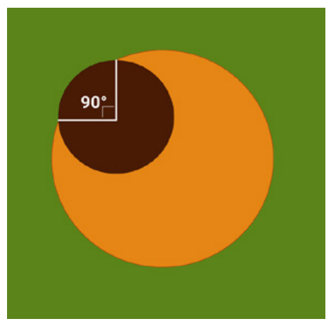
A 90-degree breakout occurs when the section of the via, drifted outside the pad, is 1.4 times the radius of the via in length. This is allowed in class 2 boards as long as the conductor junction width is wide enough.

A 180-degree breakout is when the width of the breakout is the same as the diameter of the via. This is not allowed in an IPC class 2 nor class 3 PCBs.

For board designs that cannot tolerate breakouts, the annular ring needs to be a minimum of 5 mils or greater. This is displayed in the graph given below:

breakout-vs-annular-ring-width

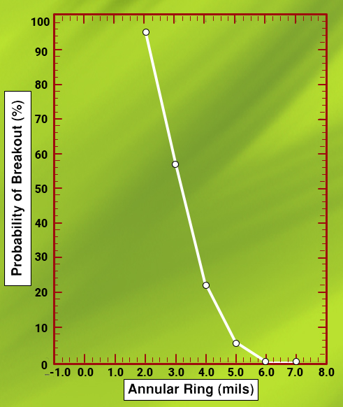
Boards with annular ring widths lesser than 5mils have a higher probability of breakout ranging from 22% for a 4 mil ring width to a maximum of 98% probability for a ring width of 2 mil. So board designers will have to use microvias of 5 mil with a 5% probability of breakout.

» MORE

One-stop PCB assembly services, capabilities, and testing

We source components from chip manufacturers across the globe, including Mouser, Digi-Key, Arrow Electronics and others. We also warehouse a significant inventory of common parts. If we cannot source a specific component, our engineers will make recommendations for fair-price alternatives. Get started now.


IPC Class 3 Design Guide - Cover Image

IPC Class 3 Design Guide

8 Chapters - 23 Pages - 35 Minute Read
What's Inside:
  • IPC guidelines for manufacturing defects
  • IPC standards for assembly processes
  • Common differences between the classes
  • IPC documents to set the level of acceptance criteria
LEARN PCB
PCB Manufacturing
PCB Assembly
PCB Design and Layout
PCB Basics
Vias, Drilling & Throughplating
Mechanics
Surface
SMD
Quality
SPECIFICATIONS
PCB Fabrication
STANDARDS & POLICY
PCB Ordering
Policy

Sierra Circuits is
headquartered in Silicon Valley.
We welcome visitors at
our 70,000 sqft facility,
located at 1108 West Evelyn Avenue
in Sunnyvale, California.
Book a tour with an account manager today!
Let us introduce you to one of the most innovative communities of engineers and designers in the world.
We can help you plan your project from design to assembled board.

Manufacturing Equipment at Sierra Circuits

Our 70,000 sqft state-of-the-art campus in the heart of Silicon Valley contains the most advanced equipment required for the manufacture and assembly of your PCBs. Whether you’re looking for standard quick turn PCBs or boards with the tightest tolerances, made from exotic metals, there’s a reason Sierra Circuits leads the industry in quality and performance.

PCBs manufactured and assembled in the United States

Turn-times as fast as 1 day.

Sierra Circuits can manufacture your PCB and have it expedited to you within 24 hours.

Full turnkey boards, with assembly and components in as fast as 5 days.

Get an Instant, Itemized Quote

Talk to a Sierra Circuits PCB Expert today

24 hours a day, 7 days a week.

Call us: +1 (800) 763-7503
Book a Meeting with a Sales Rep
Email us: through our Customer Care form