


Contents

On-demand webinar
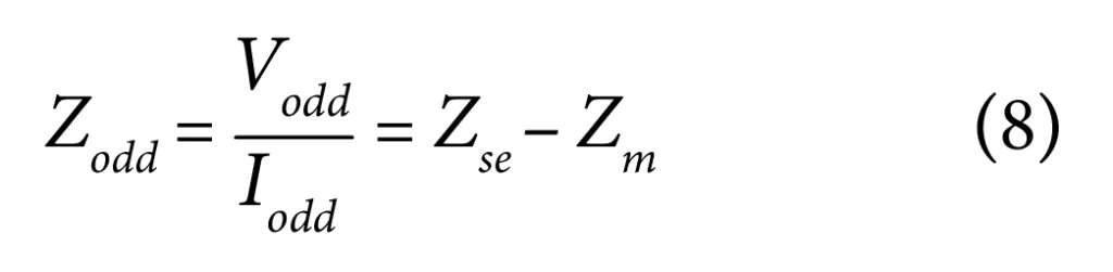
How Good is My Shield? An Introduction to Transfer Impedance and Shielding Effectiveness
by Karen Burnham
This article, written by Atar Mittal, the General Manager of our Design and PCB Assembly Divisions, will go over the characteristics and parameters of differential pairs in PCB transmission lines.
How to design differential pairs in PCB transmission lines
What is a single-ended line?
In our PCB transmission line article, we established that a single-ended transmission line can be modeled as follows:
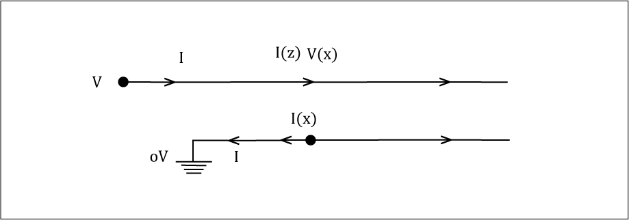
The relation between the voltage and current at any point on the line is given by:

Where ‘Z0’ is the characteristic (or instantaneous) impedance of the line. For a lossless or almost lossless line, we saw that ‘Z0’ is given by:

Where ‘L0’ and ‘C0’ are respectively the inductance and capacitance per unit length (pul) of the line.
PCB Transmission Line eBook
5 Chapters - 20 Pages - 25 Minute ReadWhat's Inside:
- What is a PCB transmission line
- Signal speed and propagation delay
- Critical length, controlled impedance and rise/fall time
- Analyzing a PCB transmission line
Download Now
Differential pair line
A pair of lines can be modeled as follows:
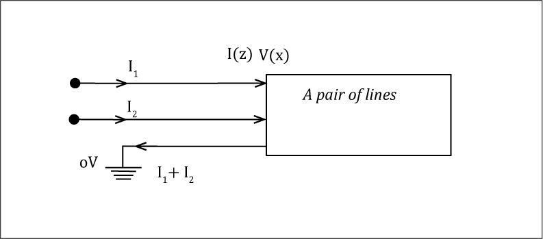
We will assume here that both of the lines of the pair are identical and uniform. And that they have the same separation from each other along the entire length of the line. These are precisely the characteristics of a pair of lines to be designated as a differential pair.
When we have a pair of lines close to each other, it is fair to say that the presence of a current in line 2 will induce some voltage in line 1, and a current in line 1 will induce some voltage in line 2. Thus, the voltage ‘V1’ at line 1 will not only depend on the current ‘I1’ in line 1 (through the impedance ‘Z0’ of line 1). It will also depend on the current ‘I2’ in line 2 through coupling or mutual impedance ‘Zm’ between lines 1 and 2. The following equation can express this situation:
 between differential lines")
Where ‘Zse’ is the characteristic impedance of line 1 and ‘Zm’ is the mutual or coupling impedance between line 1 and line 2.
Coupling between the two lines
Similarly, for line 2 (of the differential pair), being identical to line 1, we can write the following equation:
The mutual impedance ‘Zm’ arises because of the coupling between the two lines:
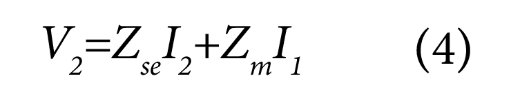
And the most important coupling agents are ‘Lm’, the mutual inductance pul, and ‘Cm’, the mutual capacitance pul between lines 1 and 2.
The closer the two lines are to each other, the greater is the coupling between them. If the separation ‘S’ between the lines is reduced, the values of all three parameters – ‘Lm’, ‘Cm’, and ‘Zm’ – increase.
The equations (3) and (4) are true for any point on line 1 and the corresponding point on line 2. And for a uniform differential pair, the ‘Zse’ and ‘Zm’ have the same value at every location along the differential pair.
Coupling coefficient
Since ‘Zm’ provides the magnitude of the signal voltage coupled from one line to another, as compared to the signal contributed through its own ‘Zse’, we may define the ratio ‘Zm/Zse’ as the coupling coefficient between the two lines of a differential pair:


What are differential and common-mode signals?
Odd and even modes
Let ‘V1’ and ‘V2’ be the signal voltages and ‘I1’ and ‘I2’ be the signal currents in the two lines of a differential pair characterized by impedances ‘Zse’ and ‘Zm’. These six quantities are related through equations (3) and (4).
The difference in signal voltage ‘V1’ and ‘V2’ is called the differential signal ‘Vdiff’. Half of it is also called the odd mode signal:

The average value of ‘V1’ and ‘V2’ is the common mode signal ‘Vcom’. It is also called the even mode signal:

From 5 and 6, we can express ‘V1’ and ‘V2’ in terms of ‘Vdiff’ and ‘Vcom’ as follows:

These equations indicate the universal fact that any two arbitrary signal values ‘V1’ and ‘V2’ can always be expressed as and therefore analyzed in terms of a common (or even) mode signal and a differential (or odd) mode signal.
Furthermore, the equations (7a) and (7b) also allow us to think that ‘Vcom’ or ‘Veven’ part of the signals in ‘V1’ and ‘V2’ are a kind of ‘’bias’’ on top of which the differential mode (or odd mode) signals ‘+Vodd’ and ‘-Vodd’ ride to result in ‘V1’ and ‘V2’. This viewpoint is the most important aspect of differential signaling analysis.
Propagating time: Varying signals
At this point, before we proceed further in our conceptual analysis, let’s keep in mind that the use of transmission lines – single-ended or differential – is to propagate time-varying signals – usually high-speed digital signals or high-frequency analog signals – from one place to another. It is time-varying signals that constitute information. Static voltages and currents do not have any information.
Therefore, looking at equations (7a) and (7b) above, we need to emphasize that ‘Vcom’ (or ‘Veven’) is only a de-bias voltage on the two lines of a differential pair. The main signal is the differential signal (‘V1 – V2’). Half of which is added to line 1, usually called the positive line. It is identified by the suffix ‘+’ or ‘P’ in the name of the signal on it. The other half is subtracted from line 2, usually called the negative line and identified by the suffix ‘-‘ or ‘N’ in the name of the signal on it, to constitute ‘V1’ and ‘V2’ at the signal transmitter end.
At the destination
At the destination, the two lines go to the inputs of a differential receiver, which detects the difference (‘V1 – V2’) in the amplitude of the signals on the two lines as the true signal. Thereby, in the process, rejecting any common mode signal, deliberate AC bias, and/or common mode noise.
This ability of rejecting the common mode signal and thus any common mode noise in differential signaling makes it far superior to single-ended signaling, where there is no way to separate the noise from the actual signal.
Having stated this, we may be tempted to think that we need to analyze deeper only the differential or odd mode and ignore the common mode. But let’s not forget that as signals propagate on the lines, they are susceptible to all kinds of noise that gets superimposed on them. This may affect signal integrity adversely. Therefore, while differential pair lines’ response to the differential (ie. odd) part of the signal is our main concern, we must also analyze the differential pair’s response to the common (or even) mode signal.
How to analyze differential and odd-mode signals?
We will now analyze the differential pair when we have sent only odd-mode signals, without any common-mode part.
In this case, since ‘Vcom = Veven = 0’, we have from (7a) and (7b):

Since the lines are identical, we will have ‘I2 = -I’ so that ‘I1 + I2 = 0’. Thus, there will be zero current in the return path.
Equation (3) or (4) now gives us:

We, as usual, define the ratio of ‘Vodd/Iodd’ as the odd-mode impedance of the line:
Now ‘Zm = K.Zse’ where ‘K’ is the coefficient of coupling.

From this, it is clear that odd mode impedance is less than the single-ended impedance ‘Zse’ of the single line and greater the ‘Zm’ (or coupling between the two lines of the pair) is, the lesser will ‘Zodd’ be from ‘Z0’.

High-Speed PCB Design Guide
8 Chapters - 115 Pages - 150 Minute ReadWhat's Inside:
- Explanations of signal integrity issues
- Understanding transmission lines and controlled impedance
- Selection process of high-speed PCB materials
- High-speed layout guidelines
Download Now
What is differential impedance?
The differential impedance is the impedance seen by a purely differential (ie, odd mode) signal over a differential pair. As:

Thus, the differential impedance is twice the odd-mode impedance. Or the odd mode impedance is half of the differential impedance.
Most often, the only specified requirement of a differential pair is its differential impedance. Typical values for most common differential signal types are 90-ohm differential, 100-ohm differential, or 120-ohm differential. In some cases, we can also use 75-ohm differential impedance.
Differential pairs: even or common mode?
Let’s now take the case when both the lines of the differential pair are excited by a common signal:

Since ‘V1 – V2 = 0’, there is no differential mode signal. As ‘V1 = V2’, ‘I1 = I2’, and the equations (3) and (4) become:

Therefore, we can define the even mode impedance ‘Zeven’ as the ratio of the even mode voltage to the even mode current in each line:

As:

And the common mode signal current in the differential pair is ‘I1 + I2 = 2I1’ so that the common mode impedance of the differential pair is:

Thus, the common mode impedance of the differential pair is half of the even mode impedance of one line. It basically equals two even-mode impedances in parallel.
From equation (10), it is clear that ‘Zeven’ is greater than ‘Zse’. The greater the coupling between the two lines of the pair is, the larger ‘Zeven’ will be compared to ‘Zse’.

Recap: Odd and even mode impedances
Odd and even mode impedances of a differential pair of lines are fundamental characteristics of the pair. We can evaluate all other impedances from their values, as illustrated below:
Since:


To these, we can add:

Detailed analysis of a differential pair in terms of line inductances and capacitances:
The analysis of a lossless single-ended transmission line was done using the following circuit model for an infinitesimally small line of length ‘delta x’:
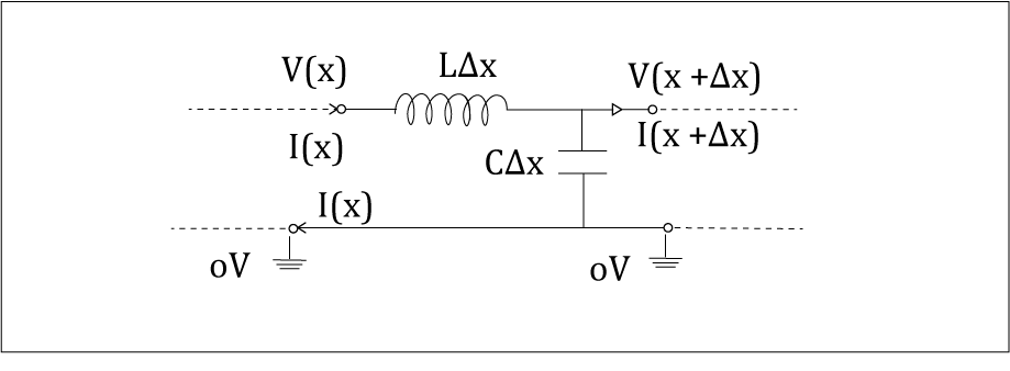
Here, ‘L’ and ‘C’ are respectively the inductance and capacitance per unit length of the line. After analysis, we had derived that the characteristic (or instantaneous) impedance of the line at a point was given by:

And the propagation delay ‘Pd’ was given by:

We can now apply the above model and results to the analysis of the lines of a differential pair in terms of inductances and capacitances involved. And we are assuming that lines as such that the conductor resistances (‘Rs’) and dielectric conductances (‘Gs’) can be neglected for the impedance and propagation delay purposes. This will be the case at practical frequencies of interest.
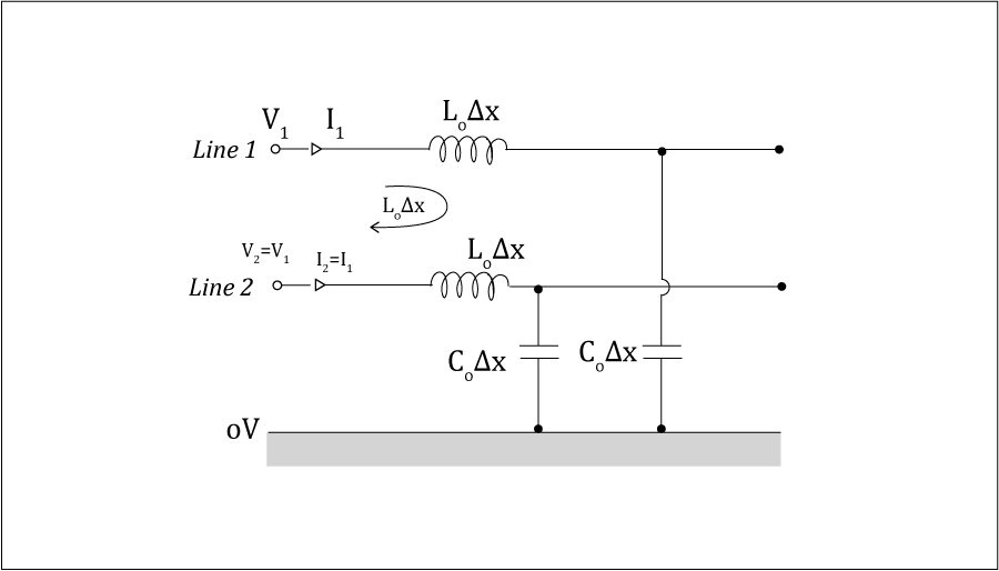
The following diagram gives the circuit model of an infinitesimally small length of a differential pair line:
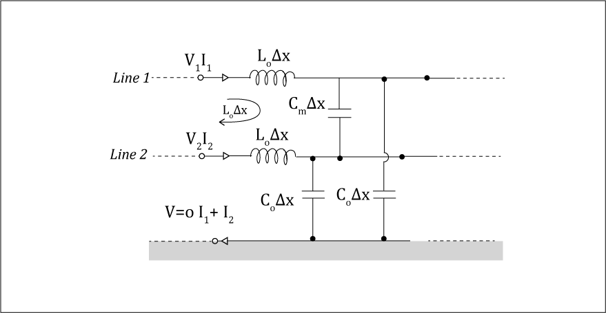
Here ‘L0’ and ‘C0’ are respective by the inductance and capacitance of each line per unit length. ‘Lm’ is the mutual inductance per unit length between line 1 and line 2. ‘Cm’ is the capacitance per unit length between line 1 and line 2.
Case 1: Odd mode (purely differential signal)
Here ‘V2 = -V1’ and ‘I2 = -I1’. Thus, no current flows in the return path. ‘Cm delta x’ can be considered as two capacitors, each of value ‘2Cm delta x’, in series, whose center point is at zero potential. (That is because of the potential division between two equal capacitors.) Thus, the equivalent circuit of the above in odd mode becomes:
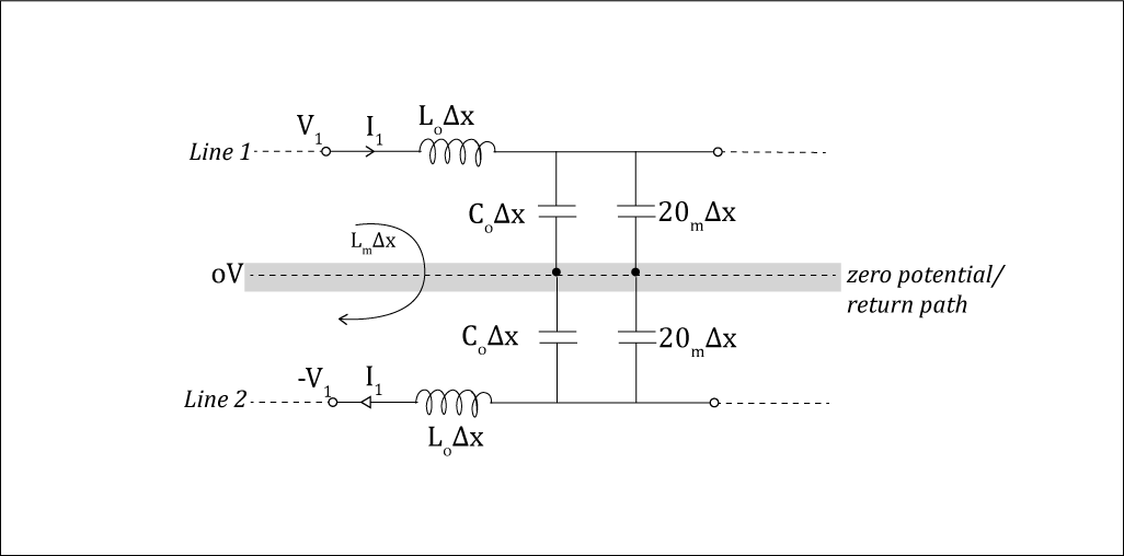
Let’s look at line 1 (the line 2 case is exactly similar).
The inductive voltage in line 1 will consist of two parts. One due to ‘I’, flowing through ‘L0 delta x’. The other one due to ‘I2 = -I1’, flowing through ‘Lm delta x’. These can be equivalently stated as due to ‘I’, flowing through (L0–Lm) delta x. Thus, the effective inductance per unit length of line 1 in odd mode, denoted by ‘Lodd’, will be given by:

And the effective capacitance between line 1 and zero potential line is ‘(C0 + 2Cm) delta x’. Thus, the odd mode line capacitance per unit length is:

By definition and similar to results derived in the case of the single-ended line, the odd mode characteristic impedance is given by:

And the propagation delay per unit length for odd-mode signals is given by:

This is the propagation delay per unit length that will take place for the purely differential part of the signal. The point to also remember here is that the odd mode or purely differential signal’s electromagnetic waves exist largely in and around the space between the two lines. And they are relatively less affected by the reference or ground planes.
Case 2: Even mode (purely common mode signal)
In this case, ‘V2 = V1’ and as the two lines of the pair are identical, ‘I1 = I2’. Since ‘V1 = V2’, the capacitance ‘Cm’ between the two lines will not affect the currents in the two lines. It can therefore be ignored, leading to the following equivalent circuit:
Let’s look at line 1 (the line 2 case is identical).
The inductive voltage in line 1 will be contributed by ‘I1’, flowing in ‘L0 delta x’. And by ‘I2 = I1’’, flowing in ‘Lm delta x’. This is equivalent to saying ‘I1’ flowing through ‘(L0 + Lm) delta x’. Therefore, the effective inductance per unit length of either line in even mode will be:

And the effective capacitance per unit length of either line in even mode will be:

Therefore, the even mode impedance of either line will be given by:

And the propagation delay per unit length for even-mode signals is given by:

Equations (13c) and (14c) clearly indicate that ‘Zeven’ is greater than ‘Zodd’. From theory, it is also known that ‘Lm’ is less than ‘L0’ and ‘Cm’ is less than ‘C0’.
‘Zse’, ‘Zm’, and ‘K’ in terms of ‘L0’, ‘C0’, ‘Lm’, ‘Cm’
Using equations (12), (13), and (14), we have:

Some words about ‘Zse’
‘Zse’ is the single-ended impedance of either of the two lines in the presence of the other line. It is not exactly the same as the characteristic impedance. The presence of the second line somewhat reduces the impedance. The more coupled (or closer) the two lines are, ‘Zse’ will become a little less.
It is important to note that ‘Zse’ does not change much if the coupling between the two lines is not high. Or if we can make the separation between the two lines greater than the maximum conductor width or dielectric height between the signal layer and the closest ground/reference plane.
i.e., ‘Zse’ is relatively the same if the separation is greater than the maximum signal trace width, dielectric height between the signal layer and the nearest reference plane.
Further, ‘Zse’ is not approximate equal to ’L0/C0’ but is nearer to ’L0/(C0+Cm)’. This may appear surprising at first glance, but that is the case.
It is not out of place to define a few new terms:

‘KL’ and ‘KC’ can be called the inductive and capacitive coupling coefficients, respectively. Using these, we can write equation (15) as:

Since ‘KL’ and ‘KC’ are less than 1, and for most practical cases will be significantly less than 1, we can retain only the first-order terms so that:

If we compare Equation (18a) with (8a) and (18b) with (10a), it is easy to conclude that:

And:

It is worth mentioning here that in most practical cases of stripline differential pairs, the inductive coupling coefficient ‘KL’ and the capacitive coupling coefficient ‘KC’ are nearly equal if the dielectric constants of the PCB materials above and below the signal layer are nearly equal.
Two crosstalk-related parameters
Here, we would also like to define two more parameters, NEXT and FEXT:

NEXT is called the nearest crosstalk coefficient. FEXT is called the far-end crosstalk coefficient. These parameters are important in crosstalk analysis when of two nearby lines, one is the main signal line and the other is the quiet line on which we wish to determine the crosstalk voltage induced due to signal voltage on the main line. We will develop this point in the next article about crosstalk analysis in detail.
For more design information, check with our DESIGN SERVICE team.
Differential Pair eBook
3 Chapters - 18 Pages - 30 Minute ReadWhat's Inside:
- Differential and common mode signals
- Differential impedance
- Even and common modes
- The physical parameters
Download Now
About the author: Atar Mittal is the Director and General Manager of the design and assembly division at Sierra Circuits. He is responsible for the design and development of strategies and process automation tools for complex printed circuit boards and assemblies. Atar is also currently engaged in the development of productivity tools for electronics designers that would have a tremendous impact on shortening the development time.
About Atar Mittal : Atar Mittal is the General Manager and Director of the Design and Assembly Sierra Circuits division. He has a degree in Electrical Engineering from IIT Kharagpur and has worked in the electronics industry for over three decades.


Start the discussion at sierraconnect.protoexpress.com